I haven't had time or motivation to dig into the shoot-through analysis described in the previous few posts, but I thought I'd look into another aspect of the same problem: the push-pull drivers.
These come in two basic categories: inverting and non-inverting. I then have two implementations of each, depending on whether the high-side driver is an FDV301 or a BSS83 FET. Each of these requires separate evaluation. In this post we'll look at only the inverting flavors, leaving the non-inverting flavors for the next post.

Experiments with the world's first microprocessor
and other electronic explorations
Sunday, January 17, 2016

Monday, January 11, 2016
Whittling down the suspect count
All I wanted to do as a first pass was to identify those that need a closer look and which don't. But since I don't have an index of which FETs are used for what purpose I had to take a look at all 105 FETs connected to Vdd to identify them. Searching for a FET by part identifier and recognizing one of the common configurations I listed in the previous post only took a few seconds per part.
It turns out there are eight tri-state drivers, reducing the number of suspect circuits from 20 to 12. Here's the list:
It turns out there are eight tri-state drivers, reducing the number of suspect circuits from 20 to 12. Here's the list:
- T0667 -- ACC D0 input latch precharge
- T0668 -- ACC D1 input latch precharge
- T0669 -- ACC D2 input latch precharge
- T0670 -- ACC D3 input latch precharge
- T0857 -- I/O D3 output(?) precharge
- T0858 -- I/O D2 output(?) precharge
- T0859 -- I/O D1 output(?) precharge
- T0860 -- I/O D0 output(?) precharge
- T1333 -- unknown
- T1477 -- unknown
- T1510 -- ALU D1 precharge
- T1512 -- ALU D3 precharge
Sunday, January 10, 2016
Looking for more potential short-circuits
Although the shoot-through problem in the incrementer will be fairly easy to address, I'm concerned that similar situations could exist elsewhere. I consulted with Lagos Kintli, the author of the awesome 4004 simulator, about modifying it to automatically detect these situations. We've concluded that it's not technically feasible, but I might be able to analyze the internal state log the simulator already provides.
This got me thinking about the scope of the problem. For this problem to occur, there must be an active pull-up transistor with the drain connected to Vdd. This can be determined by searching the simulator's netlist; there are 104 of them. Of these:
 All of the above have been analyzed. Although it's possible, perhaps even likely, that there may be brief transients as the push-pull drivers switch state, these will be extremely brief; unlike the problem in the incrementer which persists for as long as CLK1 is high.
That leaves20 12 potential problems to be reviewed. That's a manageable number for a manual search.
This got me thinking about the scope of the problem. For this problem to occur, there must be an active pull-up transistor with the drain connected to Vdd. This can be determined by searching the simulator's netlist; there are 104 of them. Of these:
- 58 are used in push-pull drivers (see below).
- 12 are used in Read Precharge circuits in the Instruction Pointer array.
- 8 are used in Read Precharge circuits in the Scratch Pad array.
- 6 are used in the IP Incrementer; one of these is a problem.
An undetermined number8 are used in Tri-state push-pull drivers.
That leaves
Friday, January 1, 2016
A second i4004 design flaw?
The designers of the Intel 4004 CPU were innovative and talented, but like all humans they make mistakes. One, affecting the Instruction Pointer counter, I described in a previous post. The more I look at this, the more I think this is a second mistake.
Wednesday, December 30, 2015
Incrementer shoot-through analysis
The problem I'm investigating occurs when the incrementer circuit attempts to pull a signal high and low at the same time. This happens whenever these conditions are all true:
- CLK1 == 1'b1
- D[0:3] == 4'b1111
- M12+M22+CLK1~(M11+M12) == 1'b1
Tuesday, December 29, 2015
Shooting the Incrementer
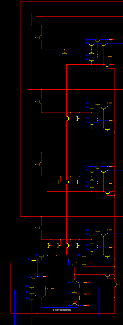
The next oddity I though I'd investigate is the always-on pass transistor in the CLK1 signal in the IP incrementer. You can spot it on the far right edge and near the bottom of the picture below; look for the FET with its gate hard-wired to Vdd.
 When I built my IP board I blindly followed the i4004 design, and the incrementer seemed to work during my testing described in my post Like a Phoenix back in September 2012. But this FET has always been a source of confusion. Why would the chip designers do this?
I dreamed up various theories. The one that seemed most likely was a critical timing condition, as a signal passing through such a FET would incur some small delay. Another thought was some sort of ringing in the chip, with this FET acting as a snubber. I thought about putting my IP board on the bench and see what effect this FET might have, but I'd be probing blindly.
So what function does this signal (N0325 in the simulator) perform? It seems to cause some signals to be driven high that may or may not be pulled to ground later, a common dynamic logic technique used in the DRAM array and elsewhere. But while stepping the simulator through the first carry operation (00F to 010) I noticed something strange: some of the signals go into "undefined" states (circuits colored gray in the picture). This means that they're being driven both high and low at the same time. This can result in "shoot-through", where Vdd is connected to Vss through a low-resistance path. Ouch!
This seems to be the case in the screen capture I posted above. This particular capture occurred at cycle 1586 but it's not a unique situation. Yet I can't imagine Intel could meet power dissipation targets with large shoot-through currents. So what's going on?
Maybe there isn't a low-resistance path. That might happen if the FET driving the signal high isn't turned on fully. How would you keep this FET from turning on fully? You'd lower the gate voltage. That pass transistor might have that effect; the output voltage would be limited to a maximum of Vdd - Vgs. Remember that CLK1 (and CLK2) are driven externally much closer to Vdd than other inputs. Unfortunately I really don't know the gate threshold voltage of the P-channel MOSFETs used in the real i4004.
Wouldn't I have seen signals going into undefined states in my testing? The Verilog version of the incrementer is behavioral, not gate-level, so it wouldn't have shown up there. It's not a situation I considered when testing the actual IP board, and my logic analyzer's buffer limitations prevented me from seeing the carry out of the first nibble to the second. I can't even say for sure that the nibble-carry works.
Once again, I seem to have a mystery on my hands. I'll have to put my IP board on the bench and see whether the incrementer handles carries from one nibble to the next properly. I'd like to probe the circuits that go to "undefined" states with my oscilloscope, but I'll have to give some thought to how to trigger on it.
I dreamed up various theories. The one that seemed most likely was a critical timing condition, as a signal passing through such a FET would incur some small delay. Another thought was some sort of ringing in the chip, with this FET acting as a snubber. I thought about putting my IP board on the bench and see what effect this FET might have, but I'd be probing blindly.
So what function does this signal (N0325 in the simulator) perform? It seems to cause some signals to be driven high that may or may not be pulled to ground later, a common dynamic logic technique used in the DRAM array and elsewhere. But while stepping the simulator through the first carry operation (00F to 010) I noticed something strange: some of the signals go into "undefined" states (circuits colored gray in the picture). This means that they're being driven both high and low at the same time. This can result in "shoot-through", where Vdd is connected to Vss through a low-resistance path. Ouch!
This seems to be the case in the screen capture I posted above. This particular capture occurred at cycle 1586 but it's not a unique situation. Yet I can't imagine Intel could meet power dissipation targets with large shoot-through currents. So what's going on?
Maybe there isn't a low-resistance path. That might happen if the FET driving the signal high isn't turned on fully. How would you keep this FET from turning on fully? You'd lower the gate voltage. That pass transistor might have that effect; the output voltage would be limited to a maximum of Vdd - Vgs. Remember that CLK1 (and CLK2) are driven externally much closer to Vdd than other inputs. Unfortunately I really don't know the gate threshold voltage of the P-channel MOSFETs used in the real i4004.
Wouldn't I have seen signals going into undefined states in my testing? The Verilog version of the incrementer is behavioral, not gate-level, so it wouldn't have shown up there. It's not a situation I considered when testing the actual IP board, and my logic analyzer's buffer limitations prevented me from seeing the carry out of the first nibble to the second. I can't even say for sure that the nibble-carry works.
Once again, I seem to have a mystery on my hands. I'll have to put my IP board on the bench and see whether the incrementer handles carries from one nibble to the next properly. I'd like to probe the circuits that go to "undefined" states with my oscilloscope, but I'll have to give some thought to how to trigger on it.
Sunday, November 8, 2015
The Bootstrap Load mystery solved
Subscribe to:
Posts (Atom)