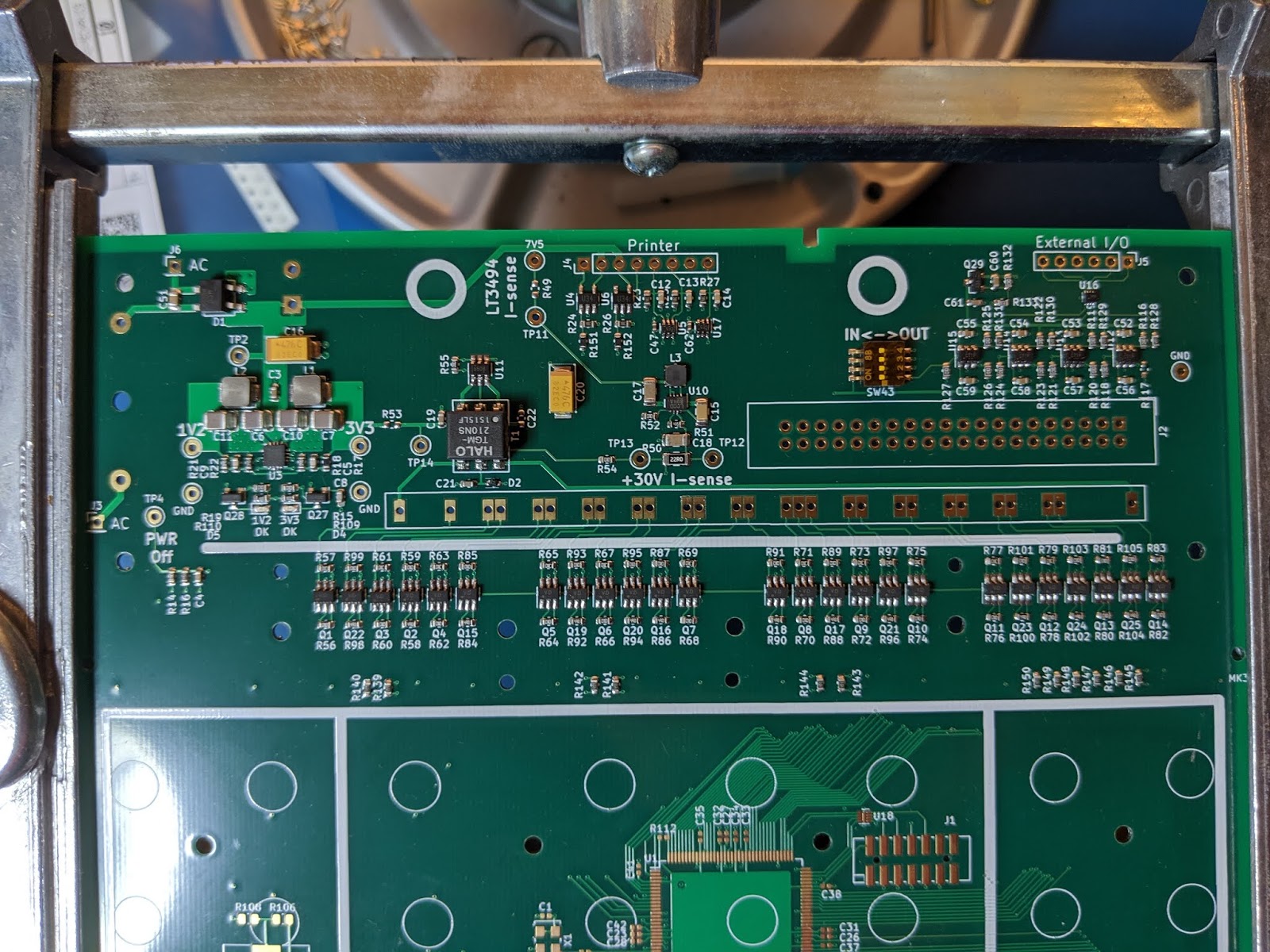
I ran my walking-one test on the Vacuum Fluorescent Display drivers. Initially I had some confusion because I'd forgotten that the VFD mounts on the bottom (keypad) side of this board, rather than the top (component) side as with my VFD driver test board. Thus the ones walked from the right side of the board as I look at it, rather than from the left as I'd intended. But the +30V boost regulator and all of the drivers are working as planned.
With this test configuration loaded I measured the supply current. While supplying 7.5V the board draws about 36 mA, and about 52 mA at 5V. That's about 270 mW, which is in the range I expected to see.

Experiments with the world's first microprocessor
and other electronic explorations
Tuesday, December 31, 2019
Monday, December 30, 2019
Found my lost electrons
To confirm my analysis, I told iMPACT to verify the contents of the Flash ROM with the image I'd previously written. This loads the JTAG-to-SPI core, which sets all the non-SPI I/O pins to PULLUP. While this was running I noted that the supply current spiked to about 200 mA. I measured the voltage on the LTC3494 and SN6505B enable pins and found them just under 3V; they need to be below 0.3V for these chips to be disabled.
Having created valid test conditions, I changed out the 100K ohm pull-down resistors on the VFD +30V boost regulator and filament transformer driver, replacing them with 750 ohm resistors. Now when I access the Flash ROM from iMPACT the ammeter now barely twitches and the enable pins sit at about 0.25V. Satisfied, I changed the pull-downs on the printer drivers circuits.
I also chased down the problems with my walking-one test of the debug interface. When I reattached the FPGA to the board after reorienting it, I didn't remove all the solder from the pads. My thinking was that since I couldn't put down new solder paste, I'd just re-heat the solder already there. The problem is that now the FPGA isn't sitting flat, and some of the pins (fingers?) didn't get soldered. The debug interface pins that were misbehaving were floating. By careful inspection I found several such pins and fixed them. Or at least I think I fixed them.
With this in mind, my next test will be to do the walking-one test on the VFD interface. This will show whether any of those pins are disconnected. I wrote the code this evening, and I'll run the test on the board in the morning.
Sunday, December 29, 2019
Where have all my electrons gone?
I think I found the reason the +30V boost regulator is getting turned on, and it isn't pretty.
Both the LTC3494 boost regulator and the SN6505 transformer driver have active-high enable inputs. The control inputs in the circuits I designed to drive the vacuum fluorescent display's grids and anodes are NPN transistors in common emitter configurations. The printer and keyclick sounder circuit inputs are N-channel FETs in common source configurations. All of these want to see inputs of no more than 0.3 to 0.5 volts to remain off.
When a Spartan 6 FPGA resets it has to load its configuration from external storage. During this period it normally configures its I/O pins with soft pull-ups. In this state, each pin could source up to 500 µA. Because this would turn on all my external circuits, I disabled this behavior by strapping the HSWAPEN configuration pin high.
Apparently I didn't notice this paragraph in application note XAPP974, Indirect Programming of SPI Serial Flash PROMs with Spartan-3A FPGAs:
With all 25 of the VFD drivers enabled, the +30V boost regulator is trying to drive 25 pull-down resistors presenting a load of about 752 ohms, and that's without the VFD itself attached. This circuit isn't intended to source 40 mA or more, and needs to be shut down to avoid damage to the circuit due to overloading.
If I disable the +30V boost regulator it doesn't matter if the VFD drivers are enabled, so I won't bother with them. Thus there are five circuits that may need to have their pull-down resistors reduced from 100K, listed here in decreasing importance:
I probably won't change the keyclick sounder driver pull-down from 100K. Doing so would reduce the draw on the +7.5V supply by 7.5 mA during Flash ROM programming, at the cost of an additional 4.4 mA from the +3V3 supply. But that extra draw on the +3V3 supply would occur any time the keyclick sound is being generated. So that's probably a bad thing, and nothing terrible will happen to the piezoelectric sounder if it's energized for a minute or so during Flash ROM programming.
Both the LTC3494 boost regulator and the SN6505 transformer driver have active-high enable inputs. The control inputs in the circuits I designed to drive the vacuum fluorescent display's grids and anodes are NPN transistors in common emitter configurations. The printer and keyclick sounder circuit inputs are N-channel FETs in common source configurations. All of these want to see inputs of no more than 0.3 to 0.5 volts to remain off.
When a Spartan 6 FPGA resets it has to load its configuration from external storage. During this period it normally configures its I/O pins with soft pull-ups. In this state, each pin could source up to 500 µA. Because this would turn on all my external circuits, I disabled this behavior by strapping the HSWAPEN configuration pin high.
Apparently I didn't notice this paragraph in application note XAPP974, Indirect Programming of SPI Serial Flash PROMs with Spartan-3A FPGAs:
Once the FPGA has been configured with the JTAG-to-SPI core, the unused I/Os are set to PULLUP, activating the internal pull-up on the I/O. The user can still pull down the I/O using a 1.1 kΩ resistor if dictated by system requirements.Gee, thanks Xilinx! Wouldn't it have been better if the JTAG-to-SPI core honored the state of the HSWAPEN input?
With all 25 of the VFD drivers enabled, the +30V boost regulator is trying to drive 25 pull-down resistors presenting a load of about 752 ohms, and that's without the VFD itself attached. This circuit isn't intended to source 40 mA or more, and needs to be shut down to avoid damage to the circuit due to overloading.
If I disable the +30V boost regulator it doesn't matter if the VFD drivers are enabled, so I won't bother with them. Thus there are five circuits that may need to have their pull-down resistors reduced from 100K, listed here in decreasing importance:
- The VFD +30V boost regulator
- The printer hammer driver
- The printer motor driver
- The VFD filament transformer drive
- The keyclick sounder drive
I probably won't change the keyclick sounder driver pull-down from 100K. Doing so would reduce the draw on the +7.5V supply by 7.5 mA during Flash ROM programming, at the cost of an additional 4.4 mA from the +3V3 supply. But that extra draw on the +3V3 supply would occur any time the keyclick sound is being generated. So that's probably a bad thing, and nothing terrible will happen to the piezoelectric sounder if it's energized for a minute or so during Flash ROM programming.
It's ALIVE!!!
Last night I created a very simple Verilog test configuration. It drives the two debug interface clock lines with true and inverted versions of the 20 MHz external clock, and then walks a single "1" bit down the length of the 32-bit debug interface data bus. It's such a trivial setup that I didn't even bother simulating it.
This morning I went down to my lab to see whether it'd load into the FPGA through the JTAG interface. As I mentioned in my post "Contemplating worst-case scenarios", this is a critical step. If I've made an error in the board layout or some minor aspect of the design, I can still test out the other areas of the system. But if I can't load a bitstream into the FPGA via the JTAG interface the only thing I could do is respin the board and hope I hadn't made any mistakes that would force me to respin it again.
This morning I went down to my lab to see whether it'd load into the FPGA through the JTAG interface. As I mentioned in my post "Contemplating worst-case scenarios", this is a critical step. If I've made an error in the board layout or some minor aspect of the design, I can still test out the other areas of the system. But if I can't load a bitstream into the FPGA via the JTAG interface the only thing I could do is respin the board and hope I hadn't made any mistakes that would force me to respin it again.
Thursday, December 26, 2019
Sanity checks are never wasted
I checked the VFD +30V boost regulator and filament driver by pulling their enable lines high with a clip lead and a 1K resistor and they looked good. With nothing left to test I sat down to populate the rest of the board.
Four hours after I started placing components I had everything picked, placed and soldered. I carried the board in its PanaVise holder from my soldering bench to my test bench and thought about what I wanted to test. I was pretty confident that everything was correct, but I decided to re-run the entire series of tests from the beginning. Everything looked good until I measured the +3V3 to ground and found an almost dead short. I thought, "What the hell?" and sat back for a moment. I couldn't see any solder bridges. I'd been so careful about the orientation of everything.
Four hours after I started placing components I had everything picked, placed and soldered. I carried the board in its PanaVise holder from my soldering bench to my test bench and thought about what I wanted to test. I was pretty confident that everything was correct, but I decided to re-run the entire series of tests from the beginning. Everything looked good until I measured the +3V3 to ground and found an almost dead short. I thought, "What the hell?" and sat back for a moment. I couldn't see any solder bridges. I'd been so careful about the orientation of everything.
Parts files
The replacement PCB for the Canon P170-DH calculator is the largest electronic hobby project I've attempted, when measured in terms of the number of distinct parts. The excellent Interactive BoM tool for KiCad makes it easier to place all the parts of a given type, but keeping track of where those parts are was becoming a bit of an ordeal.
Wednesday, December 25, 2019
Santa delivers
Santa, in the guise of a woman driving a FedEx truck, arrived Monday morning. Unfortunately I was "celebrating" another holiday tradition: I caught a cold. I really didn't feel like doing much except sleep until Tuesday, and it was late in the afternoon before I got organized.
I'd considered building one board for power subsystem testing and another fully-populated, but I realized that the large gap between the FPGA components and those further up the board would allow me to populate the upper third of the board separately.
I underestimated the time it would take to place all these components, and it was after midnight before I got everything placed. A few minutes with the hot air rework system got everything soldered in place and then I went to bed.
But first I took a picture:

This morning I inspected the results. One resistor had disappeared, possibly blown away during soldering, but otherwise it looked pretty good. I checked what I could check with an ohmmeter and found no obvious shorts.
I'd considered building one board for power subsystem testing and another fully-populated, but I realized that the large gap between the FPGA components and those further up the board would allow me to populate the upper third of the board separately.
I underestimated the time it would take to place all these components, and it was after midnight before I got everything placed. A few minutes with the hot air rework system got everything soldered in place and then I went to bed.
But first I took a picture:
This morning I inspected the results. One resistor had disappeared, possibly blown away during soldering, but otherwise it looked pretty good. I checked what I could check with an ohmmeter and found no obvious shorts.
Thursday, December 19, 2019
Thank you, FedEx!
I received my 4-layer printed circuit boards from JLCPCB today as scheduled. I put one on my bench and ran some basic checks with an ohmmeter, checking to make sure none of the power buses were shorted to ground or each other, and that they connect to the most remote devices on the board. They look great and I didn't find any electrical issues.
The solder stencil came in the same box, enclosed in a separate plastic sleeve which protects it from damage. It, too, looks great, and I very much like the protective sleeve.
I also got the notice of refund from PayPal for the scratched board: $12.66. Thank you, JLCPCB. I'm going to add them to my list of preferred vendors.
Finally, thank you DHL for delivering on schedule, even though it's a week before Christmas and I'm sure you're dealing with higher than normal volumes.
Wait... DHL? What about FedEx?
Tuesday, December 17, 2019
It was BoM Hell, but the parts are ordered
 I really need to find a parts inventory system suitable for personal use. I've been saying this for years, but this is getting difficult to manage.
This picture shows only the parts I've already accumulated for this project, not the parts I ordered this morning. So there will be more arriving.
Sunday, December 15, 2019
Scratched
I received an email from JLCPCB shortly after 3am this morning (4pm Monday in China) indicating they had a problem with one of the boards I ordered:
Thank you for your order from JLCPCB. Your order is completed now, but we regret to tell you that there is is 1 pcs less due to the scratch during the manufacturing process.
To not delay the delivery of your order, we sent those PCBs that are good out first. For the remaining quantity, we can remake and resend or refund the cost accordingly. Please kindly let us know which you prefer.
So sorry for the inconvenience caused!
Friday, December 13, 2019
Nudge... nudge...
I've been eagerly watching the progress of my PCB through JLCPCB's production process. Or not progress, I should say.
 I submitted the files Monday morning (US), which would be in the wee hours of Tuesday morning in China. When I next checked the order's status I saw that it had completed the first step of production, "MI", which appears to involve checks of the submitted Gerber files and identification of plated-through holes. With this complete I expected my order to progress rapidly, as had my previous order for the 2-layer fit-test board. But it hadn't.
 I submitted the files Monday morning (US), which would be in the wee hours of Tuesday morning in China. When I next checked the order's status I saw that it had completed the first step of production, "MI", which appears to involve checks of the submitted Gerber files and identification of plated-through holes. With this complete I expected my order to progress rapidly, as had my previous order for the 2-layer fit-test board. But it hadn't.
Monday, December 9, 2019
A day late and...
I finished routing and cleaning up the "final" four-layer replacement PCB for the Canon P170-DH calculator late last night. I didn't trust myself to submit the job properly at 2am. With the 13 hour time difference to Hong Kong it was already late Monday afternoon there, so I went to bed.
Sunday, December 8, 2019
The Fit-Test board has paid for itself
The fit-test board I had fabricated has paid for itself!
 This is the footprint for a TI TPD4F003 four-channel EMI filter with ESD protection. There are two on this board. This one protects the JTAG interface and the other protects the External I/O interface. It's a tiny little device, measuring only 1.80mm x 1.45mm, with pads on 0.40mm centers. For comparison, the pads on the JTAG connector visible in the lower right corner are on 2.00mm centers.
It's a little hard to tell because of the glare in this photo, but while the large rectangular ground pad in the middle is exposed, the four signal pads on each side are covered with solder mask. This would cause me serious trouble, as I'd have to try to scrape the solder mask off the copper pads before soldering the part in place without causing too much damage to the pads that are only 0.25mm wide. Even then I'd be soldering to bare copper rather than prepped with ENIG.
Saturday, December 7, 2019
Lessons from the Fit-Test board
I learned several things from the fit-test board, the most important of which is how to create a KiCad footprint with an NPTH (non-plated through hole). Unlike Eagle, which I recall has a "hole" tool, holes in KiCad footprints are specified by instantiating a "Pad" with a hole of the desired dimension, and setting the pad type to NPTH.
However, that isn't sufficient. You also need to change the pad size to match the hole size, otherwise the hole will have a copper annular ring of the default diameter (1.3mm diameter around my 1.0mm hole). Board houses (JLCPCB and OshPark, at least) seem to interpret this as a plated-through hole. It's also reportedly a good idea to untick the boxes for "technical layers" like solder mask.
However, that isn't sufficient. You also need to change the pad size to match the hole size, otherwise the hole will have a copper annular ring of the default diameter (1.3mm diameter around my 1.0mm hole). Board houses (JLCPCB and OshPark, at least) seem to interpret this as a plated-through hole. It's also reportedly a good idea to untick the boxes for "technical layers" like solder mask.
Thursday, December 5, 2019
Replacement PCB test-fit, Part 2
My 2-layer fit-test boards arrived today from JLCPCB in China. They were shipped in a sturdy box which fit the boards quite nicely, with sufficient bubble-wrap padding to keep them from rattling around inside the box. The boards themselves were vacuum-packed in yet more bubble-wrap so they didn't rub against the box, the outer bubble-wrap, or each other.


A cursory visual inspection didn't show any serious flaws. The worst I noted was some fine-line silkscreening had some small gaps. I'll probably fatten up the line widths to avoid this. I made no effort to move the part reference designations from where they landed when I originally placed the parts, so a lot of it is a jumbled mess or would overlap component pads, but all of it is sharp and easily readable with no apparent blobs or gaps. I'll put the boards under a microscope another time to check the pad shapes and such, but it looks pretty good under a simple magnifying lens.
Now to the three big questions:
- How well does the board fit in the P170-DH calculator shell?
- How well do the keypad contacts work?
- How well do the slide switch contacts work?
Saturday, November 30, 2019
Fit-test board fabrication progress
In addition to checking that I have the mechanical dimensions correct on my replacement PCB for the Canon P170-DH calculator, the fit-test board serves another purpose. This is the first time I've ordered a board from JLCPCB, a large Chinese fabrication house based in Hong Kong. This will give me a chance to look at the quality of their work and get a feel for the process and timing of their system.


Tuesday, November 26, 2019
Measure 17 times, fabricate twice
I've been trying to finish the routing on this board, but keep thinking "what if the holes need to be moved? So I decided to send off my current layout as a 2-layer board for fabrication. Since it's missing the inner two layers there are lots of vias that go nowhere, so I specified that it should not be electrically tested.
I decided to splurge and order it with the ENIG finish rather than HASL, even though it would more than double the cost of the board from $14 to $33. I want to try out the keypad and sliding switch contact patterns laid out on the back side of the board, and the only way I'll get a reasonable test is with the ENIG finish.
To facilitate this testing I decided to generate Gerber files with the vias un-tented. This means that there won't be solder mask over the vias, making them easier to access for testing. I should be able to hold ohmmeter probes in the via holes, or tack-solder wires to the vias.
If all goes well I should have the fit-test board in hand in a week or 10 days.
Sunday, November 24, 2019
Test-fitting the P170-DH replacement board, Part 1
I decided the easiest (and cheapest) way to validate the physical layout was to get some heavyweight paper card stock, print the layout on it, and see how well the edge cuts and holes line up. Here's what it looks like:

A couple of the holes (circled in blue pen) still seem to be a fraction of an inch off from where they should be. I'll fix those, but now I'm feeling like I should spend the $32 for a quick 2-layer board to validate the positions before I spend another $90 on a 4-layer board.
One of the things I'd been researching was how to specify the slot in the lower left corner of the original PCB for the board house I'm planning to use; apparently different houses have different ways to specify a slot. Fitting this paper analog I realized that there is no reason for that hole at all, nor the one in the lower right corner. There is nothing on either the upper or lower shell that mates with these holes, nor are they necessary for the keyboard. I'm guessing they serve some manufacturing purpose because they certainly don't serve any purpose that I can see. I'll probably just delete these two holes entirely.
Other than a couple of minor changes this is looking pretty good from a mechanical point of view.
Monday, November 11, 2019
Measure twice, fabricate once. Or twice?
I spent so much time this weekend working on the PCB layout I decided to do something a little different this evening: I printed the board layout on paper in a 1:1 scale and poked holes through the paper to see if they lined up with the holes in the original calculator PCB. Bearing in mind the last time I mis-measured before fabricating a PCB, I'd measured everything quite carefully. I was feeling quite pleased with myself until one of the holes marked on the paper didn't have a hole in the PCB beneath it. It looks like I got the horizontal position correct, but somehow I got the vertical position of that hole off by 2 mm. Oops.
Sunday, November 10, 2019
FPGA Power-On and External Reset
As I whittle down the list of things that need fixing before sending my PCB out for fabrication, I came to the question of how to make sure the FPGA resets cleanly on power-on, and how to force a reset externally.
The Xilinx Spartan 6 avoids many of the requirements for strict power-on sequencing by including an internal power-on reset circuit. This holds the reset of the FPGA circuitry in reset until all three power buses (Vccint, Vccaux, and Vcco2) reach operating levels. However, this requires the power supplies to meet certain ramp timing: the supplies must ramp up monotonically and must reach operating levels in 0.20 to 50.0 milliseconds.
The Xilinx Spartan 6 avoids many of the requirements for strict power-on sequencing by including an internal power-on reset circuit. This holds the reset of the FPGA circuitry in reset until all three power buses (Vccint, Vccaux, and Vcco2) reach operating levels. However, this requires the power supplies to meet certain ramp timing: the supplies must ramp up monotonically and must reach operating levels in 0.20 to 50.0 milliseconds.
Friday, November 8, 2019
P170-DH replacement PCB progress
As I've said before, I have to be in the right mood to do printed circuit board layout. If I try to force it I'm quite capable of staring at the problem for hours without making any progress. Fortunately, this is a hobby project and no one is looking over my shoulder. Except maybe those who read this blog.
When the proper mood strikes, though, I can make great strides in a short period. This week has been one of those periods.
When the proper mood strikes, though, I can make great strides in a short period. This week has been one of those periods.
Sunday, November 3, 2019
Video of the M-32TL printer in action
Here's a video of the M-32TL printer being driven by my Verilog driver module:
It's a hand-held cellphone video, and a bit unsteady. But you get the idea!
It's a hand-held cellphone video, and a bit unsteady. But you get the idea!
Printing using Verilog
After finishing coding and simulating the Verilog printer driver modules, it was time to test it with the real thing:

Even though I'm planning to use a Xilinx Spartan 6 on the replacement PCB in the Canon P170-DH calculator shell, I'm continuing to use the Lattice iCEblink40-HX1K development board for testing. One good reason for this is that I can buy a replacement iCEblink40 board for $40 (US) and have it delivered in a few days, while both of the Digilent reference boards I have are "retired" products and cost several hundreds of dollars each.

Even though I'm planning to use a Xilinx Spartan 6 on the replacement PCB in the Canon P170-DH calculator shell, I'm continuing to use the Lattice iCEblink40-HX1K development board for testing. One good reason for this is that I can buy a replacement iCEblink40 board for $40 (US) and have it delivered in a few days, while both of the Digilent reference boards I have are "retired" products and cost several hundreds of dollars each.
Thursday, October 31, 2019
Revised Verilog debounce module
A while back I wrote a post (here) about the Verilog module I used to debounce input pins. As I noted in a reply to that post, that module had a flaw that caused a single sample of the opposite polarity to be reported as an edge, even though the state output didn't change.
Later I found another problem. My modified Lattice iCEblink demo board has a clock frequency of 10 MHz. My Digilent Spartan 3E Starter board has a clock frequency of 50 MHz, and my Digilent Atlys board has a clock frequency of 100 MHz. There is no point in sampling the input pin at 100ns, 20ns, or 10ns intervals, as doing so would require a very long debounce FIFO. To address this I divided the system clock down to provide a clock enable input of a more reasonable 100 KHz, resulting in the input being sampled every 10 microseconds (remember, the printer position sensor signals are only asserted for 500us, and exhibit no appreciable bounce). However, this meant that the edge detection outputs on the iCEblink were asserted for 100 clock cycles, which then required the modules using the debounce module to do edge detection on the edge detection outputs. That's silly.
Later I found another problem. My modified Lattice iCEblink demo board has a clock frequency of 10 MHz. My Digilent Spartan 3E Starter board has a clock frequency of 50 MHz, and my Digilent Atlys board has a clock frequency of 100 MHz. There is no point in sampling the input pin at 100ns, 20ns, or 10ns intervals, as doing so would require a very long debounce FIFO. To address this I divided the system clock down to provide a clock enable input of a more reasonable 100 KHz, resulting in the input being sampled every 10 microseconds (remember, the printer position sensor signals are only asserted for 500us, and exhibit no appreciable bounce). However, this meant that the edge detection outputs on the iCEblink were asserted for 100 clock cycles, which then required the modules using the debounce module to do edge detection on the edge detection outputs. That's silly.
Friday, October 18, 2019
M-32TL Timing: Why three position sensors?
While reviewing my last post I realized that I'd left out an interesting behavior that happens after the printer hammer fires.
Let's look at a couple of waveforms captured using an intact P170-DH calculator. All of these are taken from the same capture, covering the printing of the first 6 characters on a line. The sensor signals are labeled based on the operation I expected when I started working with this printer rather than the nomenclature I use now. In each case I've placed cursors at the leading (falling) edges of the "Rotation Index" signal; these mark the start and end of one complete revolution of the print wheel.

Let's look at a couple of waveforms captured using an intact P170-DH calculator. All of these are taken from the same capture, covering the printing of the first 6 characters on a line. The sensor signals are labeled based on the operation I expected when I started working with this printer rather than the nomenclature I use now. In each case I've placed cursors at the leading (falling) edges of the "Rotation Index" signal; these mark the start and end of one complete revolution of the print wheel.

Monday, October 14, 2019
EP-102 to M-32TL Glue logic
The Busicom 141-PF calculator had a Shinshu Seiki (the predecessor of Epson) Model 102 drum printer. A drum printer has a cylinder (or drum) with rows of characters embossed across its width. The drum spins at relatively high speed, while a set of hammers on the other side of the paper presses the paper against the drum's surface at the right moment to print the desired characters. A full revolution of the drum is required to print all the characters on the line.
Here's a picture of a Shinshu Seiki Model 102 printer:

Since this printer can print 18 columns, it has 18 separate print hammers. Thus the i4004 software generates 18 signals in parallel using a pair of i4003 shift registers to activate the correct hammers at the correct time.
The Epson M-32TL printer, on the other hand, prints one character at a time by moving the print mechanism across the paper from right to left. Obviously some translation is required.
M-32TL Printer timing revisited
While browsing through my accumulated datasheets related to this project I found one for the Toshiba TC83230-0015 calculator chip. The information in it is sparse but it specifically mentions the Epson M31/M31A printer. The suggested system block diagram includes one tiny clue:


Saturday, September 28, 2019
More thoughts on i4004 clocking
Much of my concern, as expressed in previous posts like A clocking nightmare, have been based on the assumption that reflections on one of the two clock lines could cause multiple edges and thus multiple clocking of edge-sensitive circuits. While this would be correct with modern edge-clocked flip-flops, I don't think it applies to the original 4004 circuitry.
Monday, August 12, 2019
Fighting router's block
I've been quite busy at work -- you know, the thing that pays the bills -- so I haven't had much time to work on my hobby projects. When I have had time, I've found myself tinkering with small layout details and not making much progress in the routing of the board as a whole. I think of it as "router's block", akin to writer's block where you just can't seem to make much progress.
Rattling around in the back of my mind is still the question of how bad the clock distribution on my discrete component i4004 boards is. I'm hoping to find time to sit down at my electronics bench and really take a look at what the clock signals look like now. But how would I tell how adding a second (and, later, a third, fourth, and fifth) board would affect this?
Late one night it occurred to me that when I had the Instruction Pointer board fabricated I got two boards. The idea was to avoid a situation where I screwed up one board and had to wait for another to be fabricated and shipped from Europe, and it would serve as a reference if I wanted to check connectivity. Since the essential BSS83 MOSFET is no longer available I have little use for this second board. So why not use it to help test the clock distribution behavior!
All I need to do is mount connectors on this board and I have a ready-made second board to add to the board stack. Since I don't need this board to be functional, I can add whatever loads I might want to the clock lines and see what effects it would have while probing with my 'scope.
Now all I have to do is find the frelling thing. I've found the packaging these boards were shipped in (seven years ago!) but it's empty. I looked in all the obvious places for it, such as the box containing most of the components for this project, but thus far I haven't found it. This might actually be the incentive I need to properly organize my electronics lab.
Wednesday, July 10, 2019
Flipping the P170-DH board in KiCad
After flipping the power subsystems from the front of the board to the back and fixing up the layouts, the only parts remaining on the front of the board are the VFD, a filter capacitor, and the power fuse. Everything else is going to be mounted on the back. Thus it occurred to me that when I do most of my work with this board, I'm going to be looking at the back. That's where almost all of the components are. And once the board is mounted in the calculator's upper shell behind the keypad, the back is the only side I'll be able to see.
KiCad allows me to flip the display of the board in the pcbnew board editor. However, if I print an image of the board it's still the view from the front that gets printed. That means I'd either have to be looking at the board layout on a computer when placing parts and debugging, or mentally transpose component positions from a printed image. That didn't sound appealing.
KiCad allows me to flip the display of the board in the pcbnew board editor. However, if I print an image of the board it's still the view from the front that gets printed. That means I'd either have to be looking at the board layout on a computer when placing parts and debugging, or mentally transpose component positions from a printed image. That didn't sound appealing.
Saturday, June 22, 2019
The benefits of networking
One of the presentations I attended at KiCon 2019 was one entitled "Preserving History with KiCad" by James, the self-professed "Bald Engineer". Given my work with recreating the Intel 4004 CPU, his presentation sounded interesting to me.
Thursday, June 20, 2019
Making Xilinx ISE 14.7 run on Ubuntu 18.04
While cleaning my office I came across a timing diagram I'd drawn for an HDMI decoder I'd starting writing for the Digilent Atlys board, which has a Xilinx Spartan 6 FPGA. Curious to see how far I'd taken this project, I fired up the Xilinx ISE IDE. Or at least I tried to.
The last time I ran ISE I was running a derivative of Ubuntu 16.04. Now that I'm running a derivative of Ubuntu 18.04, ISE wouldn't run. And since ISE hasn't been updated since 2013 (and won't be), this is a problem. Here's the error message I got:
The last time I ran ISE I was running a derivative of Ubuntu 16.04. Now that I'm running a derivative of Ubuntu 18.04, ISE wouldn't run. And since ISE hasn't been updated since 2013 (and won't be), this is a problem. Here's the error message I got:
libpng warning: Application jmp_buf size changed
Thursday, June 6, 2019
Flipping the P170-DH power circuit layout
Last August I realized why some components on the original Canon P170‑DH calculator were mounted on the top of the board and some were mounted on the bottom: placing the through-hole components on top and the SMDs on the bottom allowed everything to be soldered on the bottom side of the board. That may have been a requirement, given the use of carbon tracks on the top side.
The original board used through-hole components for the power section. On my replacement board the only through-hole components are connectors, a fuse, and an electrolytic filter capacitor. None of the ICs I'm using are available in through-hole packages, and the FPGA has to be mounted on the bottom of the board because there isn't enough room to mount it other than behind the keypad.
Following the layout of the original board I'd placed the power section components on the top of the replacement PC board. Recently, though, I've reconsidered that arrangement. I'm just a bit concerned about surface-mount components already soldered on one side coming loose while later soldering the components on the other.
After making sure the schematic and board files were checked into my content management system (I use Git) I spent an evening flipping the power section circuits onto the bottom of the board. This required re-routing most of the circuits, and I took the opportunity to rearrange some of the circuits to make room for some components I hadn't placed yet. I haven't finished the re-route yet, but I'm happier than I was.
Friday, May 24, 2019
Linux CoreUtils developers break "ls"
I've been running Linux Mint 18.2 on my desktop for the last few years, and I've been pretty happy with it. However, it's based on Ubuntu 16.04, which is getting kinda long in the tooth. Specifically I found I couldn't compile the version of wxformbuilder I need for my KiCad work because it requires a newer compiler than is available for Ubuntu 16.04.
So I decided to upgrade my systems to something based on the Ubuntu 18.04 release, which is the latest long-term support release. Everything seemed to be going well until I started tried to list files in a directory. The first thing I found is that the sorting in "ls" now ignores underscores in file names.
For example, I was looking for a file named "pcb_parser.cpp" in the file listing:
pcb_layer_widget.cppWhen I reached the file named "pcbnew_config.cpp" I figured I must have missed it and scanned the list from the top again. Confused, I looked more methodically and found the names continue:
pcb_legacy_draw_utils.cpp
pcb_netlist.cpp
pcbnew_config.cpp
pcbnew.cpp
pcbnew_printout.cpp
pcbnew.cppWhat is this madness? This doesn't look like a sorted list to me.
pcbnew_printout.cpp
pcb_origin_transform.cpp
pcb_painter.cpp
pcb_parser.cpp
pcbplot.cpp
pcb_plot_params.cpp
As best I can tell, the people who maintain the core apps (like "ls") have decided to "improve" this fundamental application by changing the default sort algorithm to so-called "Natural Sorting". This means that if you have files with names from "file1" to "file20", you'll see "file10" after "file9" rather than after "file1". That's kind of a nifty trick, but the change in behavior is extremely confusing to those of us who have worked with Linux, Unix, and Unix-like systems for decades.
Apparently they also decided that underscores and spaces don't really count as a character, and file names are sorted as if they don't exist. Except when they do, because "file 13" will be sorted just before "file_13" which will come just before "file13", but after "file12". Clear?
That's all very nice. Except they decided to make "Natural Sorting" the new default behavior instead of an option you can choose. The docs say that the "-v" option turns on this behavior, but by trial and error I discovered that the "-v" option actually turns it OFF. Quite frankly, the unexpected change to a 40 year-old behavior is both unwanted and alarming.
Then I discovered something else: if you have spaces in a file name, "ls" now adds single-quote marks around the name. Like this:
pcb_plot_params.cppBut only if it's displaying on a terminal, so sometimes you see them and sometimes you don't. Again, this is the new default behavior.
'pcb plumber.cpp'
pcb_screen.cpp
You can disable this by adding either "-N" or "--literal" to the "ls" command, or by setting an environment variable in your .bashrc file:
QUOTING_STYLE=literalBut to find this you have to go looking for this in email threads and bug reports, because it's seemingly not documented elsewhere.
Many people have objected to these changes, but the CoreUtils developers don't care. I guess they want to leave their marks on the world, even if they're black marks.
Sunday, May 19, 2019
KiCad origin transforms
The problem with promising things to a project leader at a conference is that you need to deliver on those promises. Anything less and you lose credibility.
What did I promise to fix? When I started using KiCad in the spring of 2017, I whined about what I considered KiCad stupidity. I itemized seven specific complaints, some of which have since been addressed by the team of mostly-volunteer developers. After talking about it off and on for almost two years, last month I promised to fix numbers 1, 3, and 5.
I didn't spend two days in Chicago (and pay for the cost of the trip) talking with developers only to lose credibility by not following through.
Saturday, April 27, 2019
KiCon 2019: The KiCad Conference

Monday, April 1, 2019
Simulating the VFD Grid/Anode driver
 I was reading through an old posting about the VFD Grid and Anode driver circuit I'm planning to use, when it occurred to me that the resistor between the base of the PNP transistor and the collector of the NPN transistor might not be necessary. This is labeled R1 in the schematic to the right.
To calculate the desired resistance I'd done a bunch of hand calculations in my notebook, trying various combinations of target currents and resistor values. I started to do yet another with R1 set to zero when it occurred to me that this would be easier to do in simulation. At first I entered this circuit into LTspice using 2N3904 and 2N3906 transistors, as these are standard parts in the LTspice library. The simulation results matched my hand-calculated numbers, which gave me confidence that I'd done the calculations properly. I'm driving both transistors into saturation, and my turn-off times are anything but critical, so the choice of transistor isn't critical.
 Then I wondered how closely this approximation matched the real Toshiba RN4604. At first I thought this would be a challenge, as the process for creating a Spice model description for a transistor from its datasheet isn't that easy. Wouldn't it be nice if Toshiba provided a Spice model? Well, they do, and it's available for download from their website. To make it easier to probe the base current of Q1A (Q1 in the Spice schematic) I extracted the transistor models from the subcircuits that add the built-in bias resistors and substituted them into my circuit.
 My original plan had been to turn on Q1A by passing about 500 µA through its base. This was based on the spec'd saturation ICE of 5 mA with IBE of 250 µA, giving an hFE of 20. In the actual application I've found a grid draws about 6 mA and its 10K pull-down resistor will draw another 3 mA, so I doubled IBE for an ICE of 10 mA. If I eliminate R1 the base current jumps to 606 µA. But this puts almost the full 30 volts across the input (between pins 1 and 2); the datasheet graphs stop with an input voltage of 9 V. Even with the original R1 of 10K the input voltage is almost 25 V. So I'm thinking I should revisit this.
Looking at the hFE graphs I see the worst-case (at -25°C!) current gain at 30 mA is about 100. Of course this is in the transistor's linear region, but it implies that with a base current of 300 µA and a collector current of only 10 mA the thing will be saturated. So I tweaked my Spice simulation to sweep the value of R1 from 100 ohms to 150 Kohms. I graphed the base and collector currents of the transistor, along with the "input" voltage (the difference between pins 1 and 2 on the package). I also changed the collector load resistor to 1 KΩ to get about 30 mA collector current if the transistor was saturated. This would make it more obvious when decreasing the base drive would start having a significant effect on the collector current.
 The trick to interpreting these graphs is to remember that this is a PNP transistor in a common-emitter configuration, so the base and collector currents are negative. Thus a rise in the graph means less current. Also, the horizontal scale represents ohms, even though it's reported in volts. So the "100KV" tick actually represents 100 KΩ.
It's pretty obvious I don't need 500 µA of base current. In fact, it looks like I could make R1 as high as 100 KΩ and still drive this transistor into saturation. Setting R1 to 63 KΩ gives me 250 µA of base current, while 47 KΩ gives me 295 µA. I'll probably choose 47 KΩ to allow a generous margin for variations in bias resistor values, which can vary as much as ±30% in absolute value in the RN4604.
Sunday, March 17, 2019
Semi-final CCLK layout
Here's a screenshot of the current, and potentially final, layout of the FPGA configuration clock line (CCLK in the Xilinx docs, labeled CFG_SCK on my schematic and board).
 The TQFP-144 footprint in the upper left corner is U1, the Spartan 6 FPGA. The WSON-8 footprint in the lower center (with the big "9" on its heatsink pad) is U2, the S25FL128L Flash ROM. For scale, U1's pads are on 0.5mm centers, while U2's pads are on 1.27mm centers.
The CFG_SCK track is 0.3mm wide, giving it a characteristic impedance of 50 ohms.
The two large resistors near the lower left corner of U2 form the Thevenin terminator, should it be needed. They are 0603 packages due to their dissipation of 109mW when the CCLK output is driven to either rail (Vcco_2 is 3.3V). The other components around U2 are 0402 packages, including the pads for the 0 ohm jumper.
The reason I've chosen this layout is that without the jumper in place there is a minimum of disruption of the track between the FPGA and the Flash ROM. With any luck this is how it'll stay. With the jumper in place it bears a passing resemblance to the specified layout with a short 2mm stub to the ROM in the middle and the terminator at the end.

The CFG_SCK track is 0.3mm wide, giving it a characteristic impedance of 50 ohms.
The two large resistors near the lower left corner of U2 form the Thevenin terminator, should it be needed. They are 0603 packages due to their dissipation of 109mW when the CCLK output is driven to either rail (Vcco_2 is 3.3V). The other components around U2 are 0402 packages, including the pads for the 0 ohm jumper.
 |
| Xilinx UG380 Figure 2-22 |
Friday, March 15, 2019
What difference does a probe make?
When I bought my 1 GHz LeCroy digital oscilloscope in June of 2012 (omg, was it really almost 7 years ago??) it came with a set of four LeCroy PP007-WR probes. These have served me well but they have limitations. The first is that they're only rated to 500 MHz, the second is that their input capacitance is 9.5 pF.
Why on earth would that matter? After all, I'm not working with 1 GHz signals, so why would a 500 MHz limitation be a problem? And 9.5 pF is practically nothing.
Why on earth would that matter? After all, I'm not working with 1 GHz signals, so why would a 500 MHz limitation be a problem? And 9.5 pF is practically nothing.
Sunday, March 10, 2019
Experimenting with Micro-Cap
While looking for more info on IBIS I came across a mention that the free demo version of Micro-Cap from Spectrum-Soft.com would convert an IBIS file to Spice. This is true! Not only did it import the IBIS definition for the Spartan-6 CCLK output, it will also run my simulation. The free demo is cripple-ware so it runs quite slowly and has many other limitations, but it does run and is sufficient to run my tiny circuit.
Assuming the simulation is reasonably accurate, it tells me is that my previous attempts at simulation were valid: with a 50 ohm microstrip transmission line of about an inch (167ps) in length, it will act as a lumped circuit and no termination is required. In fact, with Thevenin termination the signal at the FPGA pin looks worse than the unterminated circuit due to the reduced output swing and thus narrower noise margins.
I'm still going to lay out pads for the Thevenin terminating resistors just in case, but I won't plan to install them before testing. And I definitely won't include the source termination resistor.
Unfortunately the Spice library Micro-Cap generates isn't acceptable to LTspice: there are some weirdnesses in how it names nodes. I suspect I could hand-edit them to be more standard. But what I'm really more interested in is using the tables it generates to validate my IBIS-to-Spice extractor, which I'm hoping to still finish and publish.
Converting IBIS to Spice
One of the things that has been frustrating me is my inability to properly simulate the CCLK I/O on the Spartan-6 FPGA. Many chip vendors don't want to reveal too much about the structure of their devices, so rather than giving Spice definitions for their interfaces they provide IBIS (I/O Buffer Information Specification) definitions. With the proper tools, IBIS allows for efficient simulations without having to simulate the device's entire I/O buffer circuit.
The problem is that none of the freely available Spice circuit simulators understands IBIS. Commercial simulators are available, but the cheapest one I found cost almost $300 for a 3-month license and some run into the tens of thousands of dollars.
The problem is that none of the freely available Spice circuit simulators understands IBIS. Commercial simulators are available, but the cheapest one I found cost almost $300 for a 3-month license and some run into the tens of thousands of dollars.
Thursday, March 7, 2019
CCLK Terminator Three
After much debate and vacillation, I've decided how I'm going to handle the CCLK circuit termination.
For detailed background, read my posts The CCLK Terminator and Terminator Two.
For detailed background, read my posts The CCLK Terminator and Terminator Two.
Saturday, March 2, 2019
Back to the P170-DH replacement PCB
It's been months since I worked on the replacement PCB for the P170-DH calculator. Both personal and work life has conspired to keep me away, but also I've been frustrated trying to finish the routing. Sometimes I'd open the PCB layout and stare at it for a while, then close it again having made no changes.
Recently I've been reading through this blog, and the desire rose to finish up projects I've left dangling for too long. I tried to beat down that feeling, but I think I may have failed.
Recently I've been reading through this blog, and the desire rose to finish up projects I've left dangling for too long. I tried to beat down that feeling, but I think I may have failed.
Sunday, February 24, 2019
Plagiarism
Definition of Plagiarize by Merriam-Webster
https://www.merriam-webster.com/dictionary/plagiarize
https://www.merriam-webster.com/dictionary/plagiarize
plagiarize
verb
pla·gia·rize | \ ˈplā-jə-ˌrīz also -jē-ə- \plagiarized; plagiarizingDefinition of plagiarize
: to steal and pass off (the ideas or words of another) as one's own : use (another's production) without crediting the source
: to commit literary theft : present as new and original an idea or product derived from an existing source
Subscribe to:
Posts (Atom)