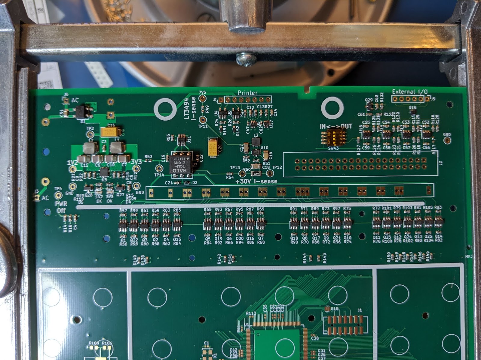
I ran my walking-one test on the Vacuum Fluorescent Display drivers. Initially I had some confusion because I'd forgotten that the VFD mounts on the bottom (keypad) side of this board, rather than the top (component) side as with my VFD driver test board. Thus the ones walked from the right side of the board as I look at it, rather than from the left as I'd intended. But the +30V boost regulator and all of the drivers are working as planned.
With this test configuration loaded I measured the supply current. While supplying 7.5V the board draws about 36 mA, and about 52 mA at 5V. That's about 270 mW, which is in the range I expected to see.

Experiments with the world's first microprocessor
and other electronic explorations
Tuesday, December 31, 2019
Monday, December 30, 2019
Found my lost electrons
To confirm my analysis, I told iMPACT to verify the contents of the Flash ROM with the image I'd previously written. This loads the JTAG-to-SPI core, which sets all the non-SPI I/O pins to PULLUP. While this was running I noted that the supply current spiked to about 200 mA. I measured the voltage on the LTC3494 and SN6505B enable pins and found them just under 3V; they need to be below 0.3V for these chips to be disabled.
Having created valid test conditions, I changed out the 100K ohm pull-down resistors on the VFD +30V boost regulator and filament transformer driver, replacing them with 750 ohm resistors. Now when I access the Flash ROM from iMPACT the ammeter now barely twitches and the enable pins sit at about 0.25V. Satisfied, I changed the pull-downs on the printer drivers circuits.
I also chased down the problems with my walking-one test of the debug interface. When I reattached the FPGA to the board after reorienting it, I didn't remove all the solder from the pads. My thinking was that since I couldn't put down new solder paste, I'd just re-heat the solder already there. The problem is that now the FPGA isn't sitting flat, and some of the pins (fingers?) didn't get soldered. The debug interface pins that were misbehaving were floating. By careful inspection I found several such pins and fixed them. Or at least I think I fixed them.
With this in mind, my next test will be to do the walking-one test on the VFD interface. This will show whether any of those pins are disconnected. I wrote the code this evening, and I'll run the test on the board in the morning.
Sunday, December 29, 2019
Where have all my electrons gone?
I think I found the reason the +30V boost regulator is getting turned on, and it isn't pretty.
Both the LTC3494 boost regulator and the SN6505 transformer driver have active-high enable inputs. The control inputs in the circuits I designed to drive the vacuum fluorescent display's grids and anodes are NPN transistors in common emitter configurations. The printer and keyclick sounder circuit inputs are N-channel FETs in common source configurations. All of these want to see inputs of no more than 0.3 to 0.5 volts to remain off.
When a Spartan 6 FPGA resets it has to load its configuration from external storage. During this period it normally configures its I/O pins with soft pull-ups. In this state, each pin could source up to 500 µA. Because this would turn on all my external circuits, I disabled this behavior by strapping the HSWAPEN configuration pin high.
Apparently I didn't notice this paragraph in application note XAPP974, Indirect Programming of SPI Serial Flash PROMs with Spartan-3A FPGAs:
With all 25 of the VFD drivers enabled, the +30V boost regulator is trying to drive 25 pull-down resistors presenting a load of about 752 ohms, and that's without the VFD itself attached. This circuit isn't intended to source 40 mA or more, and needs to be shut down to avoid damage to the circuit due to overloading.
If I disable the +30V boost regulator it doesn't matter if the VFD drivers are enabled, so I won't bother with them. Thus there are five circuits that may need to have their pull-down resistors reduced from 100K, listed here in decreasing importance:
I probably won't change the keyclick sounder driver pull-down from 100K. Doing so would reduce the draw on the +7.5V supply by 7.5 mA during Flash ROM programming, at the cost of an additional 4.4 mA from the +3V3 supply. But that extra draw on the +3V3 supply would occur any time the keyclick sound is being generated. So that's probably a bad thing, and nothing terrible will happen to the piezoelectric sounder if it's energized for a minute or so during Flash ROM programming.
Both the LTC3494 boost regulator and the SN6505 transformer driver have active-high enable inputs. The control inputs in the circuits I designed to drive the vacuum fluorescent display's grids and anodes are NPN transistors in common emitter configurations. The printer and keyclick sounder circuit inputs are N-channel FETs in common source configurations. All of these want to see inputs of no more than 0.3 to 0.5 volts to remain off.
When a Spartan 6 FPGA resets it has to load its configuration from external storage. During this period it normally configures its I/O pins with soft pull-ups. In this state, each pin could source up to 500 µA. Because this would turn on all my external circuits, I disabled this behavior by strapping the HSWAPEN configuration pin high.
Apparently I didn't notice this paragraph in application note XAPP974, Indirect Programming of SPI Serial Flash PROMs with Spartan-3A FPGAs:
Once the FPGA has been configured with the JTAG-to-SPI core, the unused I/Os are set to PULLUP, activating the internal pull-up on the I/O. The user can still pull down the I/O using a 1.1 kΩ resistor if dictated by system requirements.Gee, thanks Xilinx! Wouldn't it have been better if the JTAG-to-SPI core honored the state of the HSWAPEN input?
With all 25 of the VFD drivers enabled, the +30V boost regulator is trying to drive 25 pull-down resistors presenting a load of about 752 ohms, and that's without the VFD itself attached. This circuit isn't intended to source 40 mA or more, and needs to be shut down to avoid damage to the circuit due to overloading.
If I disable the +30V boost regulator it doesn't matter if the VFD drivers are enabled, so I won't bother with them. Thus there are five circuits that may need to have their pull-down resistors reduced from 100K, listed here in decreasing importance:
- The VFD +30V boost regulator
- The printer hammer driver
- The printer motor driver
- The VFD filament transformer drive
- The keyclick sounder drive
I probably won't change the keyclick sounder driver pull-down from 100K. Doing so would reduce the draw on the +7.5V supply by 7.5 mA during Flash ROM programming, at the cost of an additional 4.4 mA from the +3V3 supply. But that extra draw on the +3V3 supply would occur any time the keyclick sound is being generated. So that's probably a bad thing, and nothing terrible will happen to the piezoelectric sounder if it's energized for a minute or so during Flash ROM programming.
It's ALIVE!!!
Last night I created a very simple Verilog test configuration. It drives the two debug interface clock lines with true and inverted versions of the 20 MHz external clock, and then walks a single "1" bit down the length of the 32-bit debug interface data bus. It's such a trivial setup that I didn't even bother simulating it.
This morning I went down to my lab to see whether it'd load into the FPGA through the JTAG interface. As I mentioned in my post "Contemplating worst-case scenarios", this is a critical step. If I've made an error in the board layout or some minor aspect of the design, I can still test out the other areas of the system. But if I can't load a bitstream into the FPGA via the JTAG interface the only thing I could do is respin the board and hope I hadn't made any mistakes that would force me to respin it again.
This morning I went down to my lab to see whether it'd load into the FPGA through the JTAG interface. As I mentioned in my post "Contemplating worst-case scenarios", this is a critical step. If I've made an error in the board layout or some minor aspect of the design, I can still test out the other areas of the system. But if I can't load a bitstream into the FPGA via the JTAG interface the only thing I could do is respin the board and hope I hadn't made any mistakes that would force me to respin it again.
Thursday, December 26, 2019
Sanity checks are never wasted
I checked the VFD +30V boost regulator and filament driver by pulling their enable lines high with a clip lead and a 1K resistor and they looked good. With nothing left to test I sat down to populate the rest of the board.
Four hours after I started placing components I had everything picked, placed and soldered. I carried the board in its PanaVise holder from my soldering bench to my test bench and thought about what I wanted to test. I was pretty confident that everything was correct, but I decided to re-run the entire series of tests from the beginning. Everything looked good until I measured the +3V3 to ground and found an almost dead short. I thought, "What the hell?" and sat back for a moment. I couldn't see any solder bridges. I'd been so careful about the orientation of everything.
Four hours after I started placing components I had everything picked, placed and soldered. I carried the board in its PanaVise holder from my soldering bench to my test bench and thought about what I wanted to test. I was pretty confident that everything was correct, but I decided to re-run the entire series of tests from the beginning. Everything looked good until I measured the +3V3 to ground and found an almost dead short. I thought, "What the hell?" and sat back for a moment. I couldn't see any solder bridges. I'd been so careful about the orientation of everything.
Parts files
The replacement PCB for the Canon P170-DH calculator is the largest electronic hobby project I've attempted, when measured in terms of the number of distinct parts. The excellent Interactive BoM tool for KiCad makes it easier to place all the parts of a given type, but keeping track of where those parts are was becoming a bit of an ordeal.
Wednesday, December 25, 2019
Santa delivers
Santa, in the guise of a woman driving a FedEx truck, arrived Monday morning. Unfortunately I was "celebrating" another holiday tradition: I caught a cold. I really didn't feel like doing much except sleep until Tuesday, and it was late in the afternoon before I got organized.
I'd considered building one board for power subsystem testing and another fully-populated, but I realized that the large gap between the FPGA components and those further up the board would allow me to populate the upper third of the board separately.
I underestimated the time it would take to place all these components, and it was after midnight before I got everything placed. A few minutes with the hot air rework system got everything soldered in place and then I went to bed.
But first I took a picture:

This morning I inspected the results. One resistor had disappeared, possibly blown away during soldering, but otherwise it looked pretty good. I checked what I could check with an ohmmeter and found no obvious shorts.
I'd considered building one board for power subsystem testing and another fully-populated, but I realized that the large gap between the FPGA components and those further up the board would allow me to populate the upper third of the board separately.
I underestimated the time it would take to place all these components, and it was after midnight before I got everything placed. A few minutes with the hot air rework system got everything soldered in place and then I went to bed.
But first I took a picture:
This morning I inspected the results. One resistor had disappeared, possibly blown away during soldering, but otherwise it looked pretty good. I checked what I could check with an ohmmeter and found no obvious shorts.
Thursday, December 19, 2019
Thank you, FedEx!
I received my 4-layer printed circuit boards from JLCPCB today as scheduled. I put one on my bench and ran some basic checks with an ohmmeter, checking to make sure none of the power buses were shorted to ground or each other, and that they connect to the most remote devices on the board. They look great and I didn't find any electrical issues.
The solder stencil came in the same box, enclosed in a separate plastic sleeve which protects it from damage. It, too, looks great, and I very much like the protective sleeve.
I also got the notice of refund from PayPal for the scratched board: $12.66. Thank you, JLCPCB. I'm going to add them to my list of preferred vendors.
Finally, thank you DHL for delivering on schedule, even though it's a week before Christmas and I'm sure you're dealing with higher than normal volumes.
Wait... DHL? What about FedEx?
Tuesday, December 17, 2019
It was BoM Hell, but the parts are ordered
 I really need to find a parts inventory system suitable for personal use. I've been saying this for years, but this is getting difficult to manage.
This picture shows only the parts I've already accumulated for this project, not the parts I ordered this morning. So there will be more arriving.
Sunday, December 15, 2019
Scratched
I received an email from JLCPCB shortly after 3am this morning (4pm Monday in China) indicating they had a problem with one of the boards I ordered:
Thank you for your order from JLCPCB. Your order is completed now, but we regret to tell you that there is is 1 pcs less due to the scratch during the manufacturing process.
To not delay the delivery of your order, we sent those PCBs that are good out first. For the remaining quantity, we can remake and resend or refund the cost accordingly. Please kindly let us know which you prefer.
So sorry for the inconvenience caused!
Friday, December 13, 2019
Nudge... nudge...
I've been eagerly watching the progress of my PCB through JLCPCB's production process. Or not progress, I should say.
 I submitted the files Monday morning (US), which would be in the wee hours of Tuesday morning in China. When I next checked the order's status I saw that it had completed the first step of production, "MI", which appears to involve checks of the submitted Gerber files and identification of plated-through holes. With this complete I expected my order to progress rapidly, as had my previous order for the 2-layer fit-test board. But it hadn't.
 I submitted the files Monday morning (US), which would be in the wee hours of Tuesday morning in China. When I next checked the order's status I saw that it had completed the first step of production, "MI", which appears to involve checks of the submitted Gerber files and identification of plated-through holes. With this complete I expected my order to progress rapidly, as had my previous order for the 2-layer fit-test board. But it hadn't.
Monday, December 9, 2019
A day late and...
I finished routing and cleaning up the "final" four-layer replacement PCB for the Canon P170-DH calculator late last night. I didn't trust myself to submit the job properly at 2am. With the 13 hour time difference to Hong Kong it was already late Monday afternoon there, so I went to bed.
Sunday, December 8, 2019
The Fit-Test board has paid for itself
The fit-test board I had fabricated has paid for itself!
 This is the footprint for a TI TPD4F003 four-channel EMI filter with ESD protection. There are two on this board. This one protects the JTAG interface and the other protects the External I/O interface. It's a tiny little device, measuring only 1.80mm x 1.45mm, with pads on 0.40mm centers. For comparison, the pads on the JTAG connector visible in the lower right corner are on 2.00mm centers.
It's a little hard to tell because of the glare in this photo, but while the large rectangular ground pad in the middle is exposed, the four signal pads on each side are covered with solder mask. This would cause me serious trouble, as I'd have to try to scrape the solder mask off the copper pads before soldering the part in place without causing too much damage to the pads that are only 0.25mm wide. Even then I'd be soldering to bare copper rather than prepped with ENIG.
Saturday, December 7, 2019
Lessons from the Fit-Test board
I learned several things from the fit-test board, the most important of which is how to create a KiCad footprint with an NPTH (non-plated through hole). Unlike Eagle, which I recall has a "hole" tool, holes in KiCad footprints are specified by instantiating a "Pad" with a hole of the desired dimension, and setting the pad type to NPTH.
However, that isn't sufficient. You also need to change the pad size to match the hole size, otherwise the hole will have a copper annular ring of the default diameter (1.3mm diameter around my 1.0mm hole). Board houses (JLCPCB and OshPark, at least) seem to interpret this as a plated-through hole. It's also reportedly a good idea to untick the boxes for "technical layers" like solder mask.
However, that isn't sufficient. You also need to change the pad size to match the hole size, otherwise the hole will have a copper annular ring of the default diameter (1.3mm diameter around my 1.0mm hole). Board houses (JLCPCB and OshPark, at least) seem to interpret this as a plated-through hole. It's also reportedly a good idea to untick the boxes for "technical layers" like solder mask.
Thursday, December 5, 2019
Replacement PCB test-fit, Part 2
My 2-layer fit-test boards arrived today from JLCPCB in China. They were shipped in a sturdy box which fit the boards quite nicely, with sufficient bubble-wrap padding to keep them from rattling around inside the box. The boards themselves were vacuum-packed in yet more bubble-wrap so they didn't rub against the box, the outer bubble-wrap, or each other.


A cursory visual inspection didn't show any serious flaws. The worst I noted was some fine-line silkscreening had some small gaps. I'll probably fatten up the line widths to avoid this. I made no effort to move the part reference designations from where they landed when I originally placed the parts, so a lot of it is a jumbled mess or would overlap component pads, but all of it is sharp and easily readable with no apparent blobs or gaps. I'll put the boards under a microscope another time to check the pad shapes and such, but it looks pretty good under a simple magnifying lens.
Now to the three big questions:
- How well does the board fit in the P170-DH calculator shell?
- How well do the keypad contacts work?
- How well do the slide switch contacts work?
Subscribe to:
Posts (Atom)