
I'd considered building one board for power subsystem testing and another fully-populated, but I realized that the large gap between the FPGA components and those further up the board would allow me to populate the upper third of the board separately.
I underestimated the time it would take to place all these components, and it was after midnight before I got everything placed. A few minutes with the hot air rework system got everything soldered in place and then I went to bed.
But first I took a picture:
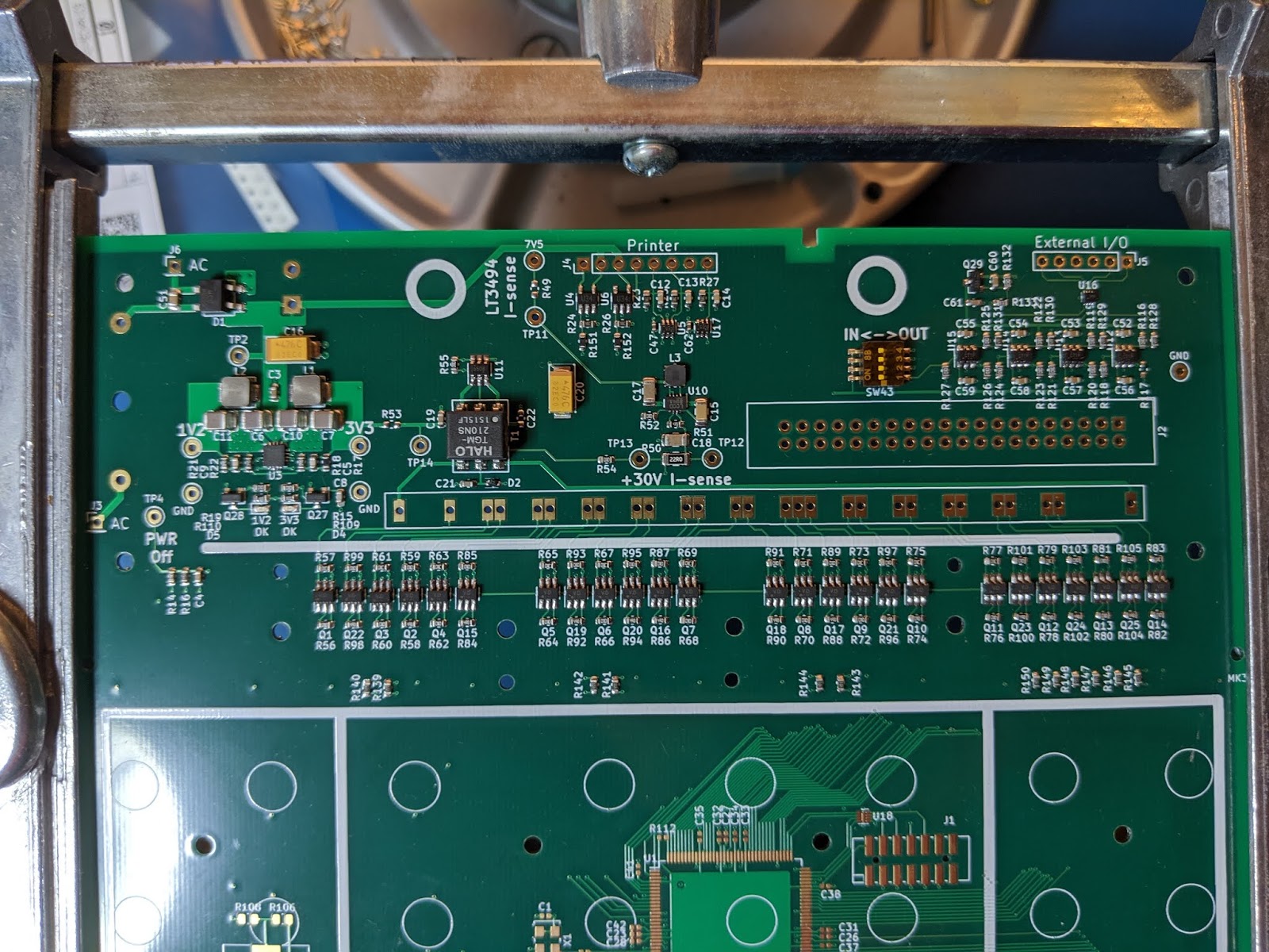
This morning I inspected the results. One resistor had disappeared, possibly blown away during soldering, but otherwise it looked pretty good. I checked what I could check with an ohmmeter and found no obvious shorts.
I shorted the +3V3 regulator's RUN input to ground to prevent it from starting and connected my bench supply to the board's unregulated DC supply bus. With some trepidation I slowly raised the supply voltage while monitoring the supply current. With the regulator held in shutdown I saw no appreciable current draw and no magic smoke appeared. Then I released the regulator's RUN input while monitoring both the supply current and the output voltage. The output rose to about 2.94V, and seemed to drift slowly upward over time. This was clearly wrong.
As this is a circuit I tested last year I knew the problem wasn't the circuit design. It should have held +3.3V ±5% regardless of time or temperature. I considered there might be an excessive load but that wasn't supported by the bench supply current which was almost nil. The +1V2 output seemed stable at +1.22V, so that side of the LTC3607 dual regulator seemed to be working properly.
Each half of the LTC3607 voltage regulator is designed to maintain its feedback input at +0.6V, using an external resistor divider to scale down the desired output voltage. The feedback voltage measured +0.6V so the regulator itself seemed to be maintaining its expected feedback, except the output voltage was too low. Thinking I might have used the wrong resistors in the feedback resistor divider I removed and measured these; they were the correct values. I replaced them anyway, just in case they were somehow defective. That didn't fix the problem. Reluctantly I decided I needed to remove the the LTC3607 -- a QFN quad leadless package with a heat sink pad -- on the assumption there was a problem under it or with the way it was mounted.
With the LTC3607 removed I looked for possible causes. The only short I noted was between two ground pads, but that could have been created as I removed the chip. I made sure all the pads were clean and shiny with no excess solder before remounting the LTC3607. I re-ran my ohmmeter checks for shorts and again found none. I slowly ramped up the input voltage while monitoring the output voltage, and when the input crossed the undervoltage lockout threshold the output jumped to +3.34V as it should have in the first place.
I'll never know for certain what the cause was, but I can think of two possibilities. One is a high-resistance leakage path between pin 15, the feedback input for the +3V3 regulator, and pin 16, the RUN input. Pin 16 is connected to the unregulated DC supply bus through a 100K resistor. With only 5µA flowing through the divider network it wouldn't take a lot of leakage to affect the feedback voltage. Such leakage from a higher voltage source would tend to cause the feedback voltage to increase, causing the regulator to reduce its output to compensate. But it couldn't have been a dead short as this would have kept the regulator from running.
The other possibility is a short between pin 15 and pin 14, the feedback input for the +1V2 regulator. Once it turned on, the +1V2 regulator also would try to maintain this pin at +0.6V. I'm not sure what sort of weird interaction there might be between the two regulators connected in the fashion. Sometime when I'm bored I might try to run a simulation of this using LTspice, but not this week.
So... after 8 hours placing components last night and 5 hours chasing regulator problems this evening, I'm ready to move forward. I intentionally didn't install two current-sense resistors to keep the number of circuits being powered to a minimum. One resistor connects the +30V boost regulator for the VFD to the unregulated DC bus, while the other connects the VFD filament driver to the +3V3 bus. Connecting these and driving their enable lines high will allow me to test their operation. I can also test the printer driver interface by stimulating inputs and monitoring their outputs. I tested the external I/O interface earlier today between bouts of hair-pulling.
If all goes well, I'll mount the FPGA and associated components tomorrow afternoon. While populating the printer driver I found to my horror that I'd used 0402 capacitors there rather than 0603 packages, but then discovered that they really aren't much harder to place than 0603s. Which is good, because I have another 43 of them to place tomorrow, along with a bunch more 0603s.
No comments:
Post a Comment