Monday, December 19, 2016

More on the M-32TL printer

The last couple of weekends I've stolen a few hours here and there to put my logic analyzer on the M-32TL printer in the Canon P170-DH calculator I've chosen as a keyboard and printer interface to my 4004 CPU reconstruction.


Here you can see the USB logic analyzer pod on the left, and the under side of the calculator on the right. The printer is visible in the upper right corner.

This printer can print in either black (blue-ish, anyway) or red. I previously linked to a web page by Arne Rossius with his analysis of the similar M-31A printer, but of course it gave no hints as to how the shift to red worked. By recording the signals received from the position sensor and the signals driving the motor and solenoid, I've been able to get a better idea how this printer works.

Although I found the pinout to be the same as described in the M-31A, I disagree with Arne's description of the function of the position sensor signals.

PinFunction
1Solenoid -
2Solenoid +
3Motor +
4Motor -
5Solenoid index
6Rotation index
7Sensor common
8Character index

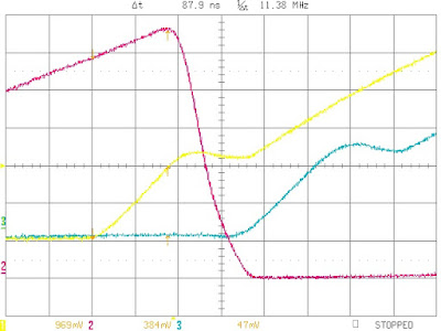
In the P170-DH, pins 2 (Solenoid +) and 3 (Motor +) are connected to the unregulated positive supply, which seems to provide a bit under 8 VDC. Pin 7 (Sensor common) is connected to ground, while pins 5, 6, and 8 are pulled to a logic "high" through resistors and debounced with an RC network. When a sensor contact connects with the conductive pattern etched on the sensor disc it pulls the logic input low.

Here's where my analysis differs: When pin 8 goes low, the printer wheels are approaching the next character. If pin 6 is also low it's the first character in the sequence given below, else it's the next one in the sequence. If this character is to be printed the solenoid is activated when pin 5 next goes low and remains activated until pin 5 goes low again.

Why not just use pin 5 to determine the character position? It appears from the signal recordings that while the character is being printed the wheels stop moving briefly. During this time pin 5 often generates several erratic low indications, while pin 8 never does. I suspect the contact for pin 5 is just on the edge of the conductor pattern on the sensor disc and any movement of the disc causes the contact to make and break. This would result in printing errors.

It also appears that this printer can print from the "Symbols" wheel in the right-most two columns, rather than only one. I haven't seen this calculator do it yet, but the second character printed thus far has always been index 10, which is a space. There's definitely enough of a gap between the right most symbol and the first number for one if not two more characters.

Wheel Character Printed
Symbols + × ÷ Δ G M C = (space) % (red)
Numbers 0 1 2 3 4 5 6 7 8 9 , #

The third character appears to be the key to the color shift. If the number portion is to be printed in black, the third character is index 10 (a space). But if the number is to be printed in red, the third character is index 13; this also prints as a space, but all following characters are printed using the red number wheel.

Printing of a line is completed by activating the solenoid for much longer than a single character time while printing the final character. In my tests the P170-DH asserted the solenoid for just under 24ms.

At some point I'll want to disconnect this printer from the calculator board so I can test it with a PIC as a driver. The reason I haven't done so yet is I'm not sure I've learned all I can before I start disassembling it. I do have a second P170-DH, but I'd rather not have to open that one up unless I need to.

Sunday, November 27, 2016

Tweaking the FDV301N Spice model: Cgs

To improve my Spice model of the FDV301N MOSFET I need to understand a little more about how they work. A lot of the dynamic behavior can be modeled as three capacitors: Cgs, Cgd, and Cds. The complexity, as seen in the model provided by Fairchild (diagrammed in the previous post), comes from the fact that the value of Cgd changes as Vgd changes. This post focuses on measuring and modeling the simplest of these: Cgs, the capacitor between the Gate and the Source.

To make life more fun, the data sheet doesn't give the value of Cgs. They give three other values, Ciss, Coss, and Crss:


My research says that Cgs can be calculated as Cgs = Ciss - Crss, so Cgs for the FDV301N should be 8.2pF. The updated Spice model Fairchild provides models Cgs as 8.5pF, which seems close enough. But how do you compare this against the real device?

As a MOSFET is driven on with a constant-current source, its gate voltage does not rise linearly. As the drawing on the right (from ON Semiconductor publication AND9083/D) shows, Vgs behavior can be characterized in three phases. In phase A (red), the gate current is charging Cgs, but Vds has not begun changing. In phase B (blue), the transistor begins to conduct and Vds begins to drop, which means the voltage across Cgd is also changing. With the gate current being consumed charging Cgd, Vgs does not change. In phase C (green), Vds has reached its minimum (or near enough to it) and the gate current goes toward charging both Cgd and Cgs.

Long ago I created an LTspice model of a chain of FDV301N inverters for simulation testing. To this I added 10pF capacitors between the gates and ground to represent my oscilloscope probes. I also replaced the U2 device, which used the Fairchild Spice model, with the X2 device, which is based on my sub-schematic version of this same model.

How can we use this to determine whether the model's Cgs matches that of a real FDV301N? Let's look at the behavior of X1 in our inverter chain. If we pretend that the load resistor of the previous inverter (R1) is a constant-current source, we can calculate the charge and the lumped capacitance of C2 and Cgs of X1. Okay, so a resistor makes a lousy constant-current source, but the first 1V rise of an RC circuit being driven to 5V is a reasonable first approximation.

I ran a simulation, probed the S1, S2, and S3 nets, and zoomed into the area where S1 rises, S2 falls, and eventually S3 rises. Here's what it looked like:


It's hard to judge from just the graph, but the time from when S1 begins to rise until S2 begins to fall is about 88ns. This is the phase which represents Cgs charging. If our model is correct, we should see the same behavior on the breadboard:


Well, what a surprise! The simulation matches the model. This suggests that the simulation models Phase A pretty well. What happens after that, in Phase B, is not so good, but that's fodder for another post.

[Edit: I've been asked several times to email the SPICE model I used. It can be downloaded from this link.]

Monday, November 21, 2016

Another attempt at simulation

I really haven't been in the mood to finish any of the PCB layouts, but I didn't want to let this project languish untouched. One of the items on my list has been to get valid simulation results so I can predict whether my choice of pull-up resistors is valid.

In the interim there's been an update to the published Spice model for the FDV301N MOSFET. One of the changes was to change the Cgs value from 78pf to 8.5pf, which makes much more sense to me. I re-ran the simulation from June 2012, and found the new model reduced the per-stage propagation delay from about 200ns to 105ns. This is an improvement, but still longer than the 70ns or so I'm seeing on the breadboard when the effects of the scope probe loading is factored out.

I'm still comparing the simulation results with the actual tracings to understand what needs tweaking to make the simulation more accurate. To make it easier to understand this rather complex model I drew the FDV301N model using the LTspice schematic capture:


The resulting netlist differs from the original model only in comments and minor formatting; otherwise it's identical right down to the net names. I no longer wonder why simulations using this model are so slow.

In the process I think I've discovered an error: the negative output of the EDB voltage source is connected to net 0 (ground), which makes no sense given that the positive output is connected via diode D to the FET's drain pin.  It seems to me that only things related to the temperature input (net 50) should be referenced to ground. I don't think this is affecting the test simulations, since all the Source pins (net 30) are connected to ground, but it would affect some of my real circuits.

Monday, May 23, 2016

Choosing an FPGA for board six

I've been thinking a lot about a sixth board to support an FPGA to assist in debugging and emulating the rest of a complete system (like a Busicom calculator). I'll still put a connector on the I/O & Timing board so the CPU can be interfaced directly to external logic, but having the ability to access inter-board signals and emulate missing parts of the CPU seems worth the effort.

When I first started this project, I used a Xilinx Spartan-3E FPGA development board for this, but it only provided 40 I/O signals. I thought about building my own board with the same FPGA, but it seemed a bit pricey and complicated to interface (three supply voltages with rigid power-up timings, etc). Thus I looked around and found the Lattice iCE40-HX series.

In the years since I started this project, the FPGA world has changed. Xilinx came out with their Spartan-6 series, which can run with two voltage supplies without stringent order or rise-time criteria. The parts have also become denser and cheaper ($16 vs $22). The iCE40-HX4K is still a bit less than half that price ($7), but when considering the cost of the PCB and the components required to support the FPGA (voltage regulators, SPI Flash ROM, level-shifting FETs) the difference in the cost of the FPGAs is noise.

I've decided to use the Xilinx Spartan-6 LX9 (144-pin TQFP) rather than the iCE40-HX4K. Why? In a word: Tools. I'm much more familiar with the Xilinx tool chain, and the iSIM simulator runs under Linux. The Aldec simulator provided by Lattice is a fine tool, but it only runs under Windows.

I need to finish pinning out all four remaining boards before I lay out the debug board, but I'm almost finished creating the Eagle library parts I'll use, and have most of the other components selected.

Friday, April 15, 2016

M-32TL operation notes

I took a brief look at the M-32TL printer in my Canon P170-DH calculator. I haven't figured out all the details, but here's what I've learned so far.

Wednesday, April 13, 2016

A VFD module for the calculator?

One of the problems with converting a stock calculator to emulate a Busicom 141-PF is that most calculators these days max out at 12 digits, while the 141-PF was a 15-digit calculator. The example Tim McNerney gives in his PIC-based printer emulator test data is:
//                   111111 1 1
//          123456789012345 7 8
/* ============================= */
/*          3.1415926535897 x    */
/*                        2 =    */
/*          6.2831853071794   *  */
/*                               */
/*                     -456 /    */
/*                     2.37 =    */
/*         -192.40506329113   *  */
/*                               */
/* ============================= */
Thus it's not as simple as dropping a couple of digits to truncate the output to 12 digits. Nor would that account for the two special characters that appear in columns 17 and 18. One way I'm considering handling this is to replace the P170-DH's fluorescent display with an LCD module.

One I'm considering is the CFAH2002A-TMI-JT module from Crystalfontz, a company I've bought from before. This module is a negative transmissive LCD with a blue foreground and white LED backlit characters. This is important because the P170-DH has a blue-colored plastic bezel, and I think this combination is most easily viewable compared to a the typical yellow-green transflective display. It displays two lines of 20 characters each, so I could either show the last two lines printed or display status on the second line. It's fairly inexpensive at about $15, but presents some mounting challenges.


Still, the idea of using a Vacuum Fluorescent Display module has stuck in my head. Most of the VFDs I've found haven't been suitable, but I just came across the DS2029H from Noritake-Itron. Not only does this module appear to be an almost perfect fit for the P170-DH, it's less than $30 in sample quantities from the manufacturer.


Of course VFDs require some strange power supplies (+5Vdc and +35Vdc in this case) but that's manageable. This module includes a controller that looks much the same as those found in LCD modules so I don't need to deal with segment drivers and the like. They also sell VFD modules that look just like LCD modules (including one they're discontinuing that is being sold at only $18), but like the LCD modules they wouldn't fit as well.


Edited to add: I ordered a DS2029H Vacuum Fluorescent Display from Noritake-Itron Wednesday. It just shipped, so I should have something to play with next week.

Tuesday, April 12, 2016

Another reminder to myself

I was reading some old posts to this blog when I came across a good idea that I'd since forgotten: separate the external I/O driver Vdd from the internal logic Vdd. This would allow the external I/Os to be driven to 3.3V instead of 5V, easing the interface to modern electronic components such as FPGAs. I haven't tested this idea on a breadboard yet, but it seems like it ought to work. I'm writing this posting so I don't forget the idea again.

And what about the EP-102? I got it working, mostly. There's a weird hiccup that causes additional lines to be "printed" to the serial port, but I suspect that's a glitch in the test module and not the printer emulation.

I also looked at some LCD and OLED character modules. I'm torn between 20x1, 20x2, and 16x2 modules. The 20x1 would be most readable, but might not fit in the space available. A second line would allow me to display other info like the OVR indicator, along with the characters that should be in columns 17 and 18 in the case of a 16x2. I'm also somewhat constrained by the blue-colored window in the calculator's case.

Saturday, April 2, 2016

EP-102 emulation

One of my goals, like so many i4004 hobbyists, is to recreate the Busicom 141-PF calculator. This was a printing calculator, using one of the earliest small digital printers from the company that became Epson. Some have done it with a compatible printer while others have used microprocessors to scan the hammer driver outputs and convert the results to ASCII.

I'm a professional software engineer, and have been writing software since learning Fortran in 1977. While I've written a fair amount of code for hobby projects it's not something that excites me anymore. Verilog and VHDL, on the other hand, are interesting to me because they require a different mindset and I love learning new things.

So I set out to develop an EP-102 emulator that would print on the Epson M-32TL printer in the Canon P170-DH calculator that I planned to cannibalize. Since I've been unable to find a datasheet for the M-32TL, I decided to put that off a bit and generate ASCII output on a serial interface. I can also emulate the keyboard with a serial interface, allowing me to run the real 141-PF firmware in an FPGA emulating the entire system while using a PC for input and output.

There are a lot of UART implementations available in VHDL and Verilog, but I wanted to write my own. Since I'm not looking for a full 16550 emulation it only took a few evenings to code and debug, including testing it on a Spartan-6 reference board. I'd hoped to test it on the Lattice iCE40-HX8 breakout board, but I'm having a minor but blocking issue with USB configurations (udev rules to disconnect one of the FT2232H interfaces from the serial driver, if you're curious).

Then I turned to emulating the EP-102. This is a tiny drum printer with 18 columns and 13 sectors per column. From the left, the first 15 columns can print the digits 0 to 9, a decimal separator (period or "full-stop"), or a "minus" sign. The 16th column is non-printing, and the 17th and 18th columns have various special characters. (This raises a problem with my plan to use the P170-DH, as it has a 12-digit printer. Maybe I'll replace the 12-digit VFD with a 20-character LCD or LED instead.)

When Tim McNerney analyzed the 141-PF for the i4004's 35th Anniversary he included notes on the operation of the EP-102. From these I constructed a Verilog module that looks like an EP-102 on one side and outputs a stream of ASCII characters when the "paper" is advanced on the other. This took another few evenings. I still have a bug in the synchronization of the sector timing (e.g. when I try to print 1s ASCII 2s are generated) but it's getting close.

I'm thinking it might be fun to create a "141-PF on a board" using the iCE40-HX8K breakout board, so I decided to build it for the iCE40 to see how big it is. Including the EP-102 emulation, UART transmitter, and a simple test "top" module I'm using 458 of the 7680 logic cells, or about 6%. To create a full system I'll need to add a 4004 CPU, 5 4001 ROMs, 2 i4002 RAMs, 3 4003 shift registers, the UART receiver, and the as-yet unwritten ASCII-to-keyboard converter. Will it fit? Stay tuned!

Thursday, March 31, 2016

Thou shalt check up

One of the commandments that any engineer worth his salt follows is this:
Thou shalt not assume. Thou shalt check up and make damned sure.
In July 2012 I was trying to determine how many transistors of each type I should buy. At the time a BSS83 cost 27.6¢/ea when ordered in quantity, while the FDV301 cost only 4.7¢/ea. I'd discovered the FDV301 worked well in a grounded-source configuration but the gate protection diode could be a problem in other configurations. To help with the decision I created a spreadsheet. It breaks the 1749 FETs needed into three categories:
  • 1041 with the source connected to GND
  • 105 with the drain connected to VDD
  • 603 fitting neither of the above two configurations
Clearly those in the first category were a good fit for the FDV301. The drain-to-VDD configuration wasn't suitable for the FDV301 because pulling the gate to ground could forward-bias the protection diode pulling the source to ground too. But it would guarantee that the body diode would remain reverse-biased, making another FET like the DMN26 a candidate.

When I went back to this spreadsheet this morning to see how many extra BSS83s I had on hand I got a real scare. I'd settled on using the FDV301 only in the grounded-source configuration and the BSS83 for the rest. That meant I needed 1041 FDV301s and 708 BSS83s.

I only purchased 700 BSS83s. And there are no more to be had.

I have a few short strips of tape with a few extra BSS83s I bought for experimentation but haven't used, but it'd be close. If any got lost or damaged I could end up not being able to complete the project. I bought 1200 FDV301s even after having identified a suitable replacement in the DMN26, but the BSS83 was a Unicorn. What had I been thinking??

I started thinking about replacing some of the BSS83s in the second and third categories with either FDV301s or DMN26s. The reason I hadn't done so before was the difficulty in creating an automated process for identifying those that have to be a BSS83.

Then it occurred to me that I'd already looked at one such second-category situation: push-pull drivers. I'd identified 58 places where the FDV301 would work better than the BSS83. More importantly, I'd made the substitution before purchasing the FETs, meaning I actually need 1099 FDV301s and only 650 BSS83s.

Instead of being short 8 BSS83s I have 50 extra, plus any in my little strips.

I'd have trouble respinning any of the boards, but if I don't screw up I have enough. To double-check this I reran an Eagle user-language program I'd written to count components on each board. The results of an early version of this program can be seen at the end of my posting on partitioning, but that version didn't differentiate between the transistor types. The updated version does and confirms the transistor counts above.

Whew!

The demise of the BSS83

I learned yesterday that the NXP BSS83 has been discontinued  as "non-manufacturable" and is no longer available. The last order date was December 2014 and the last delivery date December 2015. When I bought components for this project my intention was to order more than enough for the complete board set, but now I'm going to have to make sure what I have on-hand is enough. Fortunately 4-terminal FETs are only required in the pass-gate configuration and a few other critical spots.

I heard this from someone who is also interested in building a discrete component version of the 4004. Welcome to my insanity, Aston!

Over the years I've come across various FETs that could be used for such a project. The BSS83 RF FET was a good choice because it has a reasonable threshold voltage and a low gate capacitance (1.5pF), though it was N-channel rather than the 4004's P-channel construction. Others I identified included the N-channel Calogic SST215 (which might be a drop-in replacement for the BSS83) and the P-channel Micrel MIC94050. Tim McNerney suggested using the P-channel dual-FET BSS84 with the two transistors wired in series source-to-source (or drain-to-drain).

Aston has started experimenting with the MIC94050, which is now manufactured by Microchip. He asked whether it would work in the bootstrap load circuit given its low on-state resistance. My answer is it depends on what you're trying to do with it. My attempt to recreate the bootstrap load circuit was only to understand why this circuit was needed and how it worked.  My test circuit added several other components including current-limiting resistors, and I was able to recreate the circuit's operation well enough to understand it.

Tim McNerney, who is far more focused on recreating the exact design than I am, told me that Federico Faggin told him not to try to recreate the bootstrap load in a discrete component implementation because he'd never be able to match the characteristics with off-the-shelf components. I concur. You  end up with a complicated circuit where a simple resistor will do the job.

Fortunately bootstrap loads aren't necessary if you use true resistors as loads, as resistors don't turn off when the voltage across them drops below a FET's turn-on threshold the way FET loads do.

What other challenges might a hobbyist face when using the MIC94050 rather than a BSS83? I'd guess speed and power consumption will be the biggest factors. The MIC94050 has an input capacitance of 600pF, compared to the BSS83's 1.5pF and the FDV301's 9.5pF. For a given load resistor value, this will greatly increase propagation delays. To put some numbers to it, let's look at the rise-times with a 4.7K load pulling up the gate of a single FET. Trc with a BSS83 is about 7ns, and with an FDV301 about 45ns. With the MIC94050 it's 2.8us, which is more than double the 1.35us cycle time of the 4004.

To achieve a 45ns rise time we'd need to use 75 ohm load resistors, which would draw 67mA when pulled low. Assuming half of the 473 resistors are being pulled low at any time that's 14 amps at 5 volts, or about 72 watts. That'd keep your hands warm in the winter!

Worse, I haven't yet identified the longest combinational path through the 4004 logic. My recreated Instruction Pointer board appears to work quite nicely with a 2.0us cycle time, with the rest of the CPU emulated by an FPGA, but I think the critical path is in the ALU circuits. Thus I'm not sure even 45ns is fast enough to achieve a 1.35us cycle time.

Also consider the drive requirements for the CLK1 and CLK2 paths. CLK1 has to drive 28 FETs in parallel, and CLK2 has to drive 51. A little math says that's 17,000pF and 31,000pF respectively. The TC4427A Power MOSFET driver I used on my FPGA interface board is specified to drive 1,000pF at 5V in about 50ns, and has performance curves that show it driving 2,200pF in about 90ns, but we're still off by a factor of about x14.

All is not lost. The leakage current in modern discrete components is a lot lower than it was early in the development of integrated circuit technology. My DRAM test circuit appeared to hold its state for several seconds, while the 4004 refreshed its IP and Scratchpad registers every 500us or so. Since running a recreated 4004 built with MIC94050s at 741KHz isn't going to be an option, take advantage of the low leakage and run the system at a (much) lower speed. That will make everything easier to work with too (not everyone can splurge on a 1GHz digital oscilloscope).

Friday, March 25, 2016

More musing on a 6th board

As I mentioned a few days ago, I'm considering a sixth board. This one would carry a modern FPGA and components and serve two purposes:
  1. An easily reconfigurable test board to allow testing of any single board or set of boards in the i4004 CPU board stack.
  2. A system emulator for the i4004 CPU board stack, emulating the rest of the components of a Busicom PF-141 calculator.

Thursday, March 24, 2016

A bigger, almost as cheap FPGA experimenter's board

When I started looking at inexpensive FPGAs reference boards a few years back one I considered was the Lattice Semiconductor iCE40-HX1K. My Verilog i4004 implementation consumes 42% of the logic cells (and more than 58% of the 1280 PLBs). I expect I could probably squeeze the emulation for a few other MCS-4 chips needed for a simple system into it, but there wouldn't be a lot of resources left for anything else. Routing in an FPGA starts to become the limiting factor at some point even when there are free logic cells (75% seems to be a commonly quoted number).

The same line of Lattice chips has 4K and 8K parts. The 4K part comes in a 144-lead TQFP with 0.5mm lead pitch, which is manageable, but the 8K only comes in BGA packages. At the time there were no reference boards for these but that's changed; there is now a breakout board for the iCE40-HX8K:


This breakout board costs only $43 makes 120 I/Os available to the experimenter.

If the 1K part and only a few I/Os suits your needs, the iCEblink board seems to have been supplanted by the iCEstick, which is not much bigger than a large memory stick. It's dirt cheap at $22.

Thursday, March 17, 2016

I/O & Timing board progress

I've made good progress on the I/O and Timing board, so I thought I'd share a screen capture of the layout. There are currently 249 unrouted signal airwires, plus another 201 to GND and 92 to VDD.

Monday, March 14, 2016

Perhaps a different calculator?

When I started this project I wanted to find a printing calculator with a keyboard that was similar in layout to that of the Busicom 141-PF to serve as an input/output device for my CPU. I vaguely remember looking specifically for calculators with 00 keys, 12-digit capability, and a "number of decimal digits" switch. After looking at a bunch of models in my local Staples office products store I chose the Canon P170-DH Printing Calculator.


A sixth board?

When I started this project I was very worried about how I'd test this thing. I didn't want to build all five boards, only to discover I'd made some major mistake that would require scrapping them and starting over. Doing so would not only take a lot of time, but between the cost of the board and the components on it, each assembled board costs around $250. Redoing one would be frustrating and annoying, but if I had to redo all five I might well drop the project.

Starting the I/O and Timing board

I figured the best way to be sure all the right components got on the I/O and Timing board was to create an Eagle project for it. So I did. And promptly realized that a lot of the Eagle configuration I'd gotten used to has to be done on a per-board basis, like trace width and via drill diameters. This is the first i4004 board I've started since late 2012, and you can forget a lot in three years.

There are three major functional groups on this board:
  1. A self-initializing 8-bit shift register that produces the one-hot CPU phase of execution signals (A12, A22, A32, M12, M22, X12, X22, X32) and the SYNC signal.
  2. The 5-bit Chip Select decoder and external output drivers (CMROM, CMRAM0 to CMRAM3). This is the chunk of logic that I moved off the ALU board.
  3. The 4-bit, tri-state, bi-directional data bus external pin I/O drivers.
I haven't made a screen shot of the layout yet. I'm at about the half-way point, with the first two groups placed and partially routed. The layout is moving so rapidly because there is a lot of repetition within each group. The shift register is essentially 8 copies of the same 1-bit pattern, with a minor variation on the first (A12) and last (X32) bits, plus some logic to generate the SYNC signal. Once I found a layout that worked well for two adjacent bits the rest follow the pattern. The five Chip Select output drivers are all the same and the decode logic has common elements. I haven't started laying out the data bus I/O drivers yet, but it will be four instances of the same layout pattern -- one for each bit -- plus a little decode logic.

I expect the parts I've already placed will shift position (and possibly rotate in the case of the Chip Select logic) to accommodate the data I/O drivers but I don't expect any problems making it all fit. This board has the fewest components of any board in the set and there's quite a bit of free space left.

Thursday, March 10, 2016

A reminder to myself

I got to thinking about the I/O and Timing board last night, and discovered I hadn't started an Eagle project for it. This is a worry, because in September 2012 I did A little re-partitioning which involved moving the ROM/RAM chip select logic and drivers off the ALU board and onto the I/O and Timing board; a board for which a project does not exist. I don't want to lose this change.

With any luck this change was just moving an entire schematic sheet from one board project to another, but I have suspicions that it involved splitting Sheet 13 of the partitioned master into two separate sheets. Since I no longer remember what did and didn't stay in the ALU project I need to go back to the partitioned master and compare that with the ALU schematics so that chunk of logic doesn't get lost when I create the IOT board project.

Wednesday, March 9, 2016

Preliminary Scratchpad placement complete

I was having trouble getting to sleep last night, so I finished placing the remaining components on the Scratchpad board. Here's a screenshot:


With plenty of free space on the board I kept the components making up the various functions grouped and separated. The DRAM array is pretty obvious. The row drivers are to its immediate right, column pre-charge above and column sense and mux below. The control and data busses are below that (on the bottom of the board, shown in blue), and the write data latches below those.

Outlined on the right edge of the array are the row read and write enable drivers, and to their right is the 3-to-8 row address decoder. Continuing to the right is the 3-bit refresh counter, with each bit outlined. Bit 0 is on the bottom and bit 2 is on the top.

The other groupings are logic functions to generate various signals such as read and write enables for the odd and even nibbles, row read and write strobes, etc. When placing these groups I worked from the output drivers back toward the input signals. I started laying them out left-to-right, but after finishing them I decided they'd work better with each group rotated 90 degrees clockwise. Originally the order of the groups was the same as in the schematic, but I've since rearranged them into what seems better from a signal routing perspective.

Speaking of routing, I also routed the refresh counters and the row decoder logic. This seemed to be the easiest way to be sure the layout was workable. There's still a lot of routing to be done: there are 639 signal airwires, plus 424 ground and 84 VDD airwires. I also need to add power decoupling capacitors, and decide whether to add provisions for charge storage capacitors in the DRAM array as I did with the IP board.

Tuesday, March 8, 2016

Scratchpad refresh counter placement

Thinking how to best pin out the rest of the inter-board connections, last night I decided I should also look at the Scratchpad board. To my surprise I discovered I really hadn't gotten much done on this when I shelved this project back in 2013. Looking back at the blog entry I wrote about Scratchpad Array Placement in August 2012 I see I'd done the placement of the rectangular DRAM array components but not much more. Almost none of the signals are routed.

Friday, February 26, 2016

Progress on the ID board

I took a look at the Instruction Decoder board this evening and discovered there were a handful of parts that not only hadn't been routed at all yet, they weren't even in a near-final placement. I really thought I'd gotten farther on this than I had.

It wouldn't show up on a screen shot so I'm not going to bother, but I juggled most of them into a reasonable layout and routed within the groups. I also took a look at what's left unconnected and, like the ALU board, switched from a 4-layer to a 6-layer stackup using the same layer assignments as the ALU.

Ratsnest now reports 16 VDD, 32 GND, and 85 other airwires. That's after I'd already routed a bunch of unconnected GND pads. Again, I'm a bit surprised these numbers, especially the number of GND airwires.

There's still some possibility that as I get close to the final routing I'll decide to go back to a 4-layer board. Since all the components except the connectors are surface-mount, I've routed as much as practical on the top layer to minimize the number of vias (and thus minimize the board area they occupy). Looking at only the bottom and inner layer there really isn't that much there. If it's practical to route the remainder using only these two, and if the power distribution will also fit, I might dispense with the extra two layers. Or maybe not.

Wednesday, February 24, 2016

Progress on the ALU board

With six copper layers to play with, routing the ALU board has gone from challenging (if not nightmarish) to relatively easy. When routing vertical traces I no longer have to consider how I'm going to get VDD to the various pads, and routing nets to the connectors is mostly a matter of keeping routing lanes free of vias to avoid having to weave around them.

Sunday, February 21, 2016

What's a couple layers among friends?

Ever notice that some projects seem most interesting when there's something else you're avoiding doing? Yeah, me too.

November 2016 will mark the 45th anniversary of the release of the Intel 4004. This is enough of a significant anniversary to make me feel a bit of a kick in the ass to complete the remaining four boards of the CPU this year.

Monday, February 1, 2016

FDV301 turn-off characteristics

At first I thought it might be illuminating to add a resistor between the source of Q5 and Vss so I could see how much current was making it from Vdd though both Q4 and Q5 to Vss. I've been playing with the results for over a week now and just couldn't come up with a consistent explanation for my results.

I take that back. I've determined that there's so much noise between Vdd and Vss alone on the solderless breadboard that attempts to measure small signals accurately is extremely difficult. This despite a generous helping of bypass capacitors ranging from 0.1uF ceramics and 10uF tantalums to 200uF electrolytics. What seems to work best is using the oscilloscope in difference mode to measure the voltage across a single resistor. This seems to null out most of the Vdd fluctuations.

Eventually I moved R4 so it sat between Q4 and Q5 and measured the voltage across it. What I see is less than 2mA (200mV across 100 ohms) through that resistor during the low-to-high output transitions, and essentially nothing during the high-to-low transitions, regardless of which FET I use for Q4. That kinda kills shoot-through current a culprit.

To try to figure out where the current is going I modified the test circuit to put R4 in series with the gate of Q4. To minimize differences between my test circuit and the actual push-pull driver I reconnected the drain of Q4 to Vdd, and the source of Q5 to Vss.

Sunday, January 17, 2016

Non-inverting Push-Pull driver characteristics

Now let's take a look at the non-inverting push-pull driver circuit. There are two significant differences. First, the inverter formed by Q3/R3 is now in the path of the low-side driver rather than the high-side driver. Second, since it's the high-side driver that needs the higher voltage provided by the bootstrap load, R2 is now 2.2K and R3 is 4.7K.

Inverting Push-Pull driver characteristics

I haven't had time or motivation to dig into the shoot-through analysis described in the previous few posts, but I thought I'd look into another aspect of the same problem: the push-pull drivers.

These come in two basic categories: inverting and non-inverting. I then have two implementations of each, depending on whether the high-side driver is an FDV301 or a BSS83 FET. Each of these requires separate evaluation. In this post we'll look at only the inverting flavors, leaving the non-inverting flavors for the next post.

Monday, January 11, 2016

Whittling down the suspect count

All I wanted to do as a first pass was to identify those that need a closer look and which don't. But since I don't have an index of which FETs are used for what purpose I had to take a look at all 105 FETs connected to Vdd to identify them. Searching for a FET by part identifier and recognizing one of the common configurations I listed in the previous post only took a few seconds per part.

It turns out there are eight tri-state drivers, reducing the number of suspect circuits from 20 to 12. Here's the list:
  • T0667 -- ACC D0 input latch precharge
  • T0668 -- ACC D1 input latch precharge
  • T0669 -- ACC D2 input latch precharge
  • T0670 -- ACC D3 input latch precharge
  • T0857 -- I/O D3 output(?) precharge
  • T0858 -- I/O D2 output(?) precharge
  • T0859 -- I/O D1 output(?) precharge
  • T0860 -- I/O D0 output(?) precharge
  • T1333 -- unknown
  • T1477 -- unknown
  • T1510 -- ALU D1 precharge
  • T1512 -- ALU D3 precharge
I recognized what some of these do from developing the Verilog implementation and I've noted as appropriate. Of course I'll still check the timing of these. I may even double-check the timing of the IP and SP column sense precharge FETs while I'm at it.

Sunday, January 10, 2016

Looking for more potential short-circuits

Although the shoot-through problem in the incrementer will be fairly easy to address, I'm concerned that similar situations could exist elsewhere. I consulted with Lagos Kintli, the author of the awesome 4004 simulator, about modifying it to automatically detect these situations. We've concluded that it's not technically feasible, but I might be able to analyze the internal state log the simulator already provides.

This got me thinking about the scope of the problem. For this problem to occur, there must be an active pull-up transistor with the drain connected to Vdd. This can be determined by searching the simulator's netlist; there are 104 of them. Of these:
  • 58 are used in push-pull drivers (see below).
  • 12 are used in Read Precharge circuits in the Instruction Pointer array.
  • 8 are used in Read Precharge circuits in the Scratch Pad array.
  • 6 are used in the IP Incrementer; one of these is a problem.
  • An undetermined number 8 are used in Tri-state push-pull drivers.
All of the above have been analyzed. Although it's possible, perhaps even likely, that there may be brief transients as the push-pull drivers switch state, these will be extremely brief; unlike the problem in the incrementer which persists for as long as CLK1 is high.

That leaves 20 12 potential problems to be reviewed. That's a manageable number for a manual search.

Friday, January 1, 2016

A second i4004 design flaw?

The designers of the Intel 4004 CPU were innovative and talented, but like all humans they make mistakes. One, affecting the Instruction Pointer counter, I described in a previous post. The more I look at this, the more I think this is a second mistake.