

Experiments with the world's first microprocessor
and other electronic explorations
Showing posts with label Spice. Show all posts
Showing posts with label Spice. Show all posts
Tuesday, January 7, 2020
Spice simulation of the External I/O
I got to wondering how accurately my "back of the envelope" calculations modeled the External I/O interface circuit. So I set it up in LTspice:


Monday, April 1, 2019
Simulating the VFD Grid/Anode driver
 I was reading through an old posting about the VFD Grid and Anode driver circuit I'm planning to use, when it occurred to me that the resistor between the base of the PNP transistor and the collector of the NPN transistor might not be necessary. This is labeled R1 in the schematic to the right.
To calculate the desired resistance I'd done a bunch of hand calculations in my notebook, trying various combinations of target currents and resistor values. I started to do yet another with R1 set to zero when it occurred to me that this would be easier to do in simulation. At first I entered this circuit into LTspice using 2N3904 and 2N3906 transistors, as these are standard parts in the LTspice library. The simulation results matched my hand-calculated numbers, which gave me confidence that I'd done the calculations properly. I'm driving both transistors into saturation, and my turn-off times are anything but critical, so the choice of transistor isn't critical.
 Then I wondered how closely this approximation matched the real Toshiba RN4604. At first I thought this would be a challenge, as the process for creating a Spice model description for a transistor from its datasheet isn't that easy. Wouldn't it be nice if Toshiba provided a Spice model? Well, they do, and it's available for download from their website. To make it easier to probe the base current of Q1A (Q1 in the Spice schematic) I extracted the transistor models from the subcircuits that add the built-in bias resistors and substituted them into my circuit.
 My original plan had been to turn on Q1A by passing about 500 µA through its base. This was based on the spec'd saturation ICE of 5 mA with IBE of 250 µA, giving an hFE of 20. In the actual application I've found a grid draws about 6 mA and its 10K pull-down resistor will draw another 3 mA, so I doubled IBE for an ICE of 10 mA. If I eliminate R1 the base current jumps to 606 µA. But this puts almost the full 30 volts across the input (between pins 1 and 2); the datasheet graphs stop with an input voltage of 9 V. Even with the original R1 of 10K the input voltage is almost 25 V. So I'm thinking I should revisit this.
Looking at the hFE graphs I see the worst-case (at -25°C!) current gain at 30 mA is about 100. Of course this is in the transistor's linear region, but it implies that with a base current of 300 µA and a collector current of only 10 mA the thing will be saturated. So I tweaked my Spice simulation to sweep the value of R1 from 100 ohms to 150 Kohms. I graphed the base and collector currents of the transistor, along with the "input" voltage (the difference between pins 1 and 2 on the package). I also changed the collector load resistor to 1 KΩ to get about 30 mA collector current if the transistor was saturated. This would make it more obvious when decreasing the base drive would start having a significant effect on the collector current.
 The trick to interpreting these graphs is to remember that this is a PNP transistor in a common-emitter configuration, so the base and collector currents are negative. Thus a rise in the graph means less current. Also, the horizontal scale represents ohms, even though it's reported in volts. So the "100KV" tick actually represents 100 KΩ.
It's pretty obvious I don't need 500 µA of base current. In fact, it looks like I could make R1 as high as 100 KΩ and still drive this transistor into saturation. Setting R1 to 63 KΩ gives me 250 µA of base current, while 47 KΩ gives me 295 µA. I'll probably choose 47 KΩ to allow a generous margin for variations in bias resistor values, which can vary as much as ±30% in absolute value in the RN4604.
Sunday, March 10, 2019
Experimenting with Micro-Cap
While looking for more info on IBIS I came across a mention that the free demo version of Micro-Cap from Spectrum-Soft.com would convert an IBIS file to Spice. This is true! Not only did it import the IBIS definition for the Spartan-6 CCLK output, it will also run my simulation. The free demo is cripple-ware so it runs quite slowly and has many other limitations, but it does run and is sufficient to run my tiny circuit.
Assuming the simulation is reasonably accurate, it tells me is that my previous attempts at simulation were valid: with a 50 ohm microstrip transmission line of about an inch (167ps) in length, it will act as a lumped circuit and no termination is required. In fact, with Thevenin termination the signal at the FPGA pin looks worse than the unterminated circuit due to the reduced output swing and thus narrower noise margins.
I'm still going to lay out pads for the Thevenin terminating resistors just in case, but I won't plan to install them before testing. And I definitely won't include the source termination resistor.
Unfortunately the Spice library Micro-Cap generates isn't acceptable to LTspice: there are some weirdnesses in how it names nodes. I suspect I could hand-edit them to be more standard. But what I'm really more interested in is using the tables it generates to validate my IBIS-to-Spice extractor, which I'm hoping to still finish and publish.
Assuming the simulation is reasonably accurate, it tells me is that my previous attempts at simulation were valid: with a 50 ohm microstrip transmission line of about an inch (167ps) in length, it will act as a lumped circuit and no termination is required. In fact, with Thevenin termination the signal at the FPGA pin looks worse than the unterminated circuit due to the reduced output swing and thus narrower noise margins.
I'm still going to lay out pads for the Thevenin terminating resistors just in case, but I won't plan to install them before testing. And I definitely won't include the source termination resistor.
Unfortunately the Spice library Micro-Cap generates isn't acceptable to LTspice: there are some weirdnesses in how it names nodes. I suspect I could hand-edit them to be more standard. But what I'm really more interested in is using the tables it generates to validate my IBIS-to-Spice extractor, which I'm hoping to still finish and publish.
Converting IBIS to Spice
One of the things that has been frustrating me is my inability to properly simulate the CCLK I/O on the Spartan-6 FPGA. Many chip vendors don't want to reveal too much about the structure of their devices, so rather than giving Spice definitions for their interfaces they provide IBIS (I/O Buffer Information Specification) definitions. With the proper tools, IBIS allows for efficient simulations without having to simulate the device's entire I/O buffer circuit.
The problem is that none of the freely available Spice circuit simulators understands IBIS. Commercial simulators are available, but the cheapest one I found cost almost $300 for a 3-month license and some run into the tens of thousands of dollars.
The problem is that none of the freely available Spice circuit simulators understands IBIS. Commercial simulators are available, but the cheapest one I found cost almost $300 for a 3-month license and some run into the tens of thousands of dollars.
Thursday, March 7, 2019
CCLK Terminator Three
After much debate and vacillation, I've decided how I'm going to handle the CCLK circuit termination.
For detailed background, read my posts The CCLK Terminator and Terminator Two.
For detailed background, read my posts The CCLK Terminator and Terminator Two.
Monday, June 11, 2018
Spice models
Every so often someone will ask for me to post the Spice models I've used (or tried to use). For some reason these requests usually get stuck in Blogger's spam quarantine, and I only notice them some weeks (sometimes months) later.
Rather than trying to keep up with these requests, I'm going to post links to these models here. Bear in mind that I didn't create these device models; I found them on the 'net. I offer no warranty on them.
Phillips (NXP) BSS83: BSS83_N.mod
Fairchild FDV301N: FDV301N.mod
Rather than trying to keep up with these requests, I'm going to post links to these models here. Bear in mind that I didn't create these device models; I found them on the 'net. I offer no warranty on them.
Phillips (NXP) BSS83: BSS83_N.mod
Fairchild FDV301N: FDV301N.mod
Eagle track length calculation errors
I decided to see if I could simulate the CLK1 and CLK2 signals on my current Instruction Pointer board using LTspice. Why these two? They're the only signals that have rapid rise times, as the others are all limited by the RC rise time curves of the pull-up resistors and the gate and drain capacitances they drive. To do this with any accuracy I needed to simulate the actual track lengths and capacitances at their ends.
Saturday, June 9, 2018
A clocking nightmare
Apparently I woo-hooed too quickly. I decided to run some simplistic simulations with LTspice to see what would happen with two boards connected to the output of a TC4427A. It wasn't good.
Tuesday, June 5, 2018
Terminator Two
Let's take another look at the termination of the transmission line for the CCLK signal. (And yes, I do like my puns.)
Ideally I'd use an IBIS simulator and the models provided by Xilinx for this purpose. Unfortunately I don't have access to one. The best I can do at the moment is some simulations with LTspice. Still, these are instructive.
Let's start with the circuit model. All of the simulations below were run with the same basic model, with some minor changes in connectivity and values as noted.
Ideally I'd use an IBIS simulator and the models provided by Xilinx for this purpose. Unfortunately I don't have access to one. The best I can do at the moment is some simulations with LTspice. Still, these are instructive.
Let's start with the circuit model. All of the simulations below were run with the same basic model, with some minor changes in connectivity and values as noted.
Sunday, November 27, 2016
Tweaking the FDV301N Spice model: Cgs
 To improve my Spice model of the FDV301N MOSFET I need to understand a little more about how they work. A lot of the dynamic behavior can be modeled as three capacitors: Cgs, Cgd, and Cds. The complexity, as seen in the model provided by Fairchild (diagrammed in the previous post), comes from the fact that the value of Cgd changes as Vgd changes. This post focuses on measuring and modeling the simplest of these: Cgs, the capacitor between the Gate and the Source.
To make life more fun, the data sheet doesn't give the value of Cgs. They give three other values, Ciss, Coss, and Crss:

My research says that Cgs can be calculated as Cgs = Ciss - Crss, so Cgs for the FDV301N should be 8.2pF. The updated Spice model Fairchild provides models Cgs as 8.5pF, which seems close enough. But how do you compare this against the real device?
 As a MOSFET is driven on with a constant-current source, its gate voltage does not rise linearly. As the drawing on the right (from ON Semiconductor publication AND9083/D) shows, Vgs behavior can be characterized in three phases. In phase A (red), the gate current is charging Cgs, but Vds has not begun changing. In phase B (blue), the transistor begins to conduct and Vds begins to drop, which means the voltage across Cgd is also changing. With the gate current being consumed charging Cgd, Vgs does not change. In phase C (green), Vds has reached its minimum (or near enough to it) and the gate current goes toward charging both Cgd and Cgs.
Long ago I created an LTspice model of a chain of FDV301N inverters for simulation testing. To this I added 10pF capacitors between the gates and ground to represent my oscilloscope probes. I also replaced the U2 device, which used the Fairchild Spice model, with the X2 device, which is based on my sub-schematic version of this same model.

How can we use this to determine whether the model's Cgs matches that of a real FDV301N? Let's look at the behavior of X1 in our inverter chain. If we pretend that the load resistor of the previous inverter (R1) is a constant-current source, we can calculate the charge and the lumped capacitance of C2 and Cgs of X1. Okay, so a resistor makes a lousy constant-current source, but the first 1V rise of an RC circuit being driven to 5V is a reasonable first approximation.
I ran a simulation, probed the S1, S2, and S3 nets, and zoomed into the area where S1 rises, S2 falls, and eventually S3 rises. Here's what it looked like:

It's hard to judge from just the graph, but the time from when S1 begins to rise until S2 begins to fall is about 88ns. This is the phase which represents Cgs charging. If our model is correct, we should see the same behavior on the breadboard:
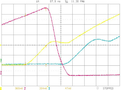
Well, what a surprise! The simulation matches the model. This suggests that the simulation models Phase A pretty well. What happens after that, in Phase B, is not so good, but that's fodder for another post.
[Edit: I've been asked several times to email the SPICE model I used. It can be downloaded from this link.]
Monday, November 21, 2016
Another attempt at simulation
I really haven't been in the mood to finish any of the PCB layouts, but I didn't want to let this project languish untouched. One of the items on my list has been to get valid simulation results so I can predict whether my choice of pull-up resistors is valid.
In the interim there's been an update to the published Spice model for the FDV301N MOSFET. One of the changes was to change the Cgs value from 78pf to 8.5pf, which makes much more sense to me. I re-ran the simulation from June 2012, and found the new model reduced the per-stage propagation delay from about 200ns to 105ns. This is an improvement, but still longer than the 70ns or so I'm seeing on the breadboard when the effects of the scope probe loading is factored out.
I'm still comparing the simulation results with the actual tracings to understand what needs tweaking to make the simulation more accurate. To make it easier to understand this rather complex model I drew the FDV301N model using the LTspice schematic capture:

The resulting netlist differs from the original model only in comments and minor formatting; otherwise it's identical right down to the net names. I no longer wonder why simulations using this model are so slow.
In the process I think I've discovered an error: the negative output of the EDB voltage source is connected to net 0 (ground), which makes no sense given that the positive output is connected via diode D to the FET's drain pin. It seems to me that only things related to the temperature input (net 50) should be referenced to ground. I don't think this is affecting the test simulations, since all the Source pins (net 30) are connected to ground, but it would affect some of my real circuits.
In the interim there's been an update to the published Spice model for the FDV301N MOSFET. One of the changes was to change the Cgs value from 78pf to 8.5pf, which makes much more sense to me. I re-ran the simulation from June 2012, and found the new model reduced the per-stage propagation delay from about 200ns to 105ns. This is an improvement, but still longer than the 70ns or so I'm seeing on the breadboard when the effects of the scope probe loading is factored out.
I'm still comparing the simulation results with the actual tracings to understand what needs tweaking to make the simulation more accurate. To make it easier to understand this rather complex model I drew the FDV301N model using the LTspice schematic capture:

The resulting netlist differs from the original model only in comments and minor formatting; otherwise it's identical right down to the net names. I no longer wonder why simulations using this model are so slow.
In the process I think I've discovered an error: the negative output of the EDB voltage source is connected to net 0 (ground), which makes no sense given that the positive output is connected via diode D to the FET's drain pin. It seems to me that only things related to the temperature input (net 50) should be referenced to ground. I don't think this is affecting the test simulations, since all the Source pins (net 30) are connected to ground, but it would affect some of my real circuits.
Subscribe to:
Posts (Atom)