
 | |
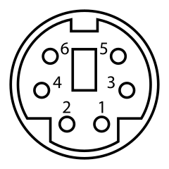
| Female PS/2 connector (front) |
My original idea was to use pins 1 and 5 as DATA and CLOCK of a conventional, unidirectional, synchronous serial interface, and use pins 2 and 6 for the reverse direction. The idea was this would be faster, more reliable, and simpler and to implement than asynchronous serial which requires a UART in my FPGAs. However, the S3E Starter kit wires pin 1 to pin 2, and pin 5 to pin 6. I'm sure the kit's designers were thinking this would allow users to talk to devices that use either pins 1/5 or pins 2/6, while only taking two of the FPGA's I/Os instead of four. But it's rather inconvenient for me.
My P170 board is set up to allow any of pins 1, 2, 5, or 6 to be configured as input or output, but the configuration is done with DIP switches rather than being controllable from the FPGA. I'm still free to use the four wires as I'd originally planned when talking to my i4004 board stack, but I'm limited to using only two when talking to the S3E Starter kit.
For testing I started by configuring the S3E to actively drive the I/O connected to the PS/2 interface's DATA pins (1 & 2) with alternating 1s and 0s. This allowed me to verify that I was driving the correct pin. On the P170 board I configured the level shifters for pins 1 and 2 as inputs and connected the PS/2 cable. I was a bit surprised to note that the SN74LVC1T45 level shifter seemed quite happy with an input that didn't quite reach its documented minimum input-high level of 3.5V; the output seems to switch state when the input crosses the 0.5 × Vccb level.
The next test was to configure the S3E as if it had open-drain outputs. This is done by setting the output buffer to pull low, then switching the buffer between active and High-Z. As expected, this resulted in a higher input-high level at the level-shifter's input pin. However the rise time was abysmal: 3 microseconds to rise above 3.5V. That suggests the cable is adding about 325pF of capacitance. A 3 microsecond rise time wouldn't be a problem at 9600bps but it becomes more of a problem as the bit rate goes up: this would narrow a "1" bit by 35% at 115200bps.
Since the level-shifter seems happy with the input levels seen when the S3E is actively driving an output high (to 3.3V), doing so would solve the slow rise-time issue. When connected to a board that has outputs that drive rail-to-rail this problem goes away entirely, regardless of whether that voltage is 3.3V or 5V.
Why do I care about high-speed serial data rates? During testing it makes sense to load the FPGA through JTAG. But once this is working reasonably well it'd be nice to be able to load a new bitfile without having to open the calculator's shell. Since the only external interface available with the calculator closed up is the serial interface, I want the option of loading the new bitfile through it. A bitfile for the LX9 is a bit over 2.7 million bits, which would take 6 minutes to load at 9600bps but only 30 seconds at 115200bps.
I have one or two more tests to do before I call the external I/O interface tested. I noticed that the DIR pin on the level shifter handling pin 2 seemed to follow its "B" input, albeit at a much reduced voltage. That isn't happening on the level shifter for pin 1. I'm thinking this might be a poor ground on this chip, so I reflowed the solder on all this chip's pins and cleaned the board of excess rosin. But I haven't retested it yet.
Another test is to verify that the P170 can send and receive on each of the external I/O pins. I may just run that test with a simple 555 timer as a signal source rather than playing with the S3E kit.
No comments:
Post a Comment