
I finally had time to directly measure the rise and fall times of the CLK1 and CLK2 signals on my i4004 Instruction Pointer board. I'm hoping this will help me decide how to distribute these signals to the five boards of my i4004 CPU.
This measurement was delayed because I updated the Linux OS on my computers since the last time I used ISE and Eagle. It took one evening to get the ISE iMPACT to run so I could program the FPGA emulating the rest of the CPU and peripheral chips. It then took a second evening to get Eagle v7 to run, as it requires shareable libraries from an older distro.
My i4004 re-creation uses a Microchip TC4427a MOSFET driver to boost the 3.3V output from the Spartan 3E FPGA to the 5.0V levels required by the discrete component boards. This chip is rated to operate with a supply voltage of 4.5V to 18V, so I'm almost at the low-end limit. As such, the voltage swings are slower than they would be at a higher voltage. Here's an excerpt from the datasheet, showing the rise and fall times with various supply voltages and load capacitances:

Since I neglected to consider the signal characteristics when I laid out the IP board, I tried using the Microchip-supplied Spice models to get an idea how the clock signals would work when feeding a collection of boards (A Clocking Nightmare). The results were not terribly encouraging.
Now, four years later, I've finally gotten around to measuring the signals on the actual IP board. First, here's the CLK1 signal as it appears on the stacked connector:

There's a bit of overshoot on the rising edge, and a bit of undershoot on the falling edge, but nothing terrible. One possible cause is the 4 inch ground lead on the oscilloscope probe.
To avoid this, I broke out my active 'scope probe. Aside from having a 1 GHz bandwidth and a fraction of the capacitance, this probe has a stiff-wire ground lead that's maybe a half-inch long. Transistor T0371, part of the Effective Address Counter, provided a good location to sample this signal, with CLK1 and GND on opposing pins of the package. Here are the rising and falling edges:
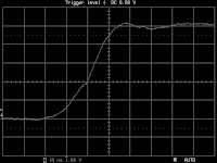

The over/undershoot observed on the connector with a passive probe is much smaller measured at this transistor, which is consistent with other transistors I checked.
This does give a clear indication of a 20 ns rise and fall (10% to 90%). As the load on this driver increases, this may stretch a bit. The CLK2 signal will eventually drive 50 FET gates; if we assume 10 pF per FET, that's a load of 500 pF. The datasheet suggests that with a load of 1000 pF the rise time will be about 50 ns. Given a pulse width of 400 ns that should be plenty fast enough. Ironically, since the i4004 design is level-sensitive rather than edge-clocked, slower is better for signal integrity.
I'm still leaning toward using different connector pins for the clock signals for each board. This would allow me to use separate source termination resistors, or even separate driver ICs, to drive each board. However, given these slow clock rise/fall times. I suspect the system will run just fine with everything connected together.
Hi Reece, your 4004 project is very impressive. I am working on a similar project since about 7 month. Is there a way to contact you? Notsure if I should post my email address here ...
ReplyDeleteThanks Klaus