
 To improve my Spice model of the FDV301N MOSFET I need to understand a little more about how they work. A lot of the dynamic behavior can be modeled as three capacitors: Cgs, Cgd, and Cds. The complexity, as seen in the model provided by Fairchild (diagrammed in the previous post), comes from the fact that the value of Cgd changes as Vgd changes. This post focuses on measuring and modeling the simplest of these: Cgs, the capacitor between the Gate and the Source.
To make life more fun, the data sheet doesn't give the value of Cgs. They give three other values, Ciss, Coss, and Crss:
My research says that Cgs can be calculated as Cgs = Ciss - Crss, so Cgs for the FDV301N should be 8.2pF. The updated Spice model Fairchild provides models Cgs as 8.5pF, which seems close enough. But how do you compare this against the real device?
 As a MOSFET is driven on with a constant-current source, its gate voltage does not rise linearly. As the drawing on the right (from ON Semiconductor publication AND9083/D) shows, Vgs behavior can be characterized in three phases. In phase A (red), the gate current is charging Cgs, but Vds has not begun changing. In phase B (blue), the transistor begins to conduct and Vds begins to drop, which means the voltage across Cgd is also changing. With the gate current being consumed charging Cgd, Vgs does not change. In phase C (green), Vds has reached its minimum (or near enough to it) and the gate current goes toward charging both Cgd and Cgs.
Long ago I created an LTspice model of a chain of FDV301N inverters for simulation testing. To this I added 10pF capacitors between the gates and ground to represent my oscilloscope probes. I also replaced the U2 device, which used the Fairchild Spice model, with the X2 device, which is based on my sub-schematic version of this same model.

How can we use this to determine whether the model's Cgs matches that of a real FDV301N? Let's look at the behavior of X1 in our inverter chain. If we pretend that the load resistor of the previous inverter (R1) is a constant-current source, we can calculate the charge and the lumped capacitance of C2 and Cgs of X1. Okay, so a resistor makes a lousy constant-current source, but the first 1V rise of an RC circuit being driven to 5V is a reasonable first approximation.
I ran a simulation, probed the S1, S2, and S3 nets, and zoomed into the area where S1 rises, S2 falls, and eventually S3 rises. Here's what it looked like:

It's hard to judge from just the graph, but the time from when S1 begins to rise until S2 begins to fall is about 88ns. This is the phase which represents Cgs charging. If our model is correct, we should see the same behavior on the breadboard:
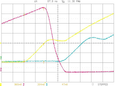
Well, what a surprise! The simulation matches the model. This suggests that the simulation models Phase A pretty well. What happens after that, in Phase B, is not so good, but that's fodder for another post.
[Edit: I've been asked several times to email the SPICE model I used. It can be downloaded from this link.]
Hi. Can you give me the pspice model of the FDV301N used in your simulations? Thank you.
ReplyDeleteEmail: vinybh@hotmail.com