When examining an existing design I try to get "into the head" of the original designers, putting myself in their shoes facing the same design questions. This often helps me understand why they made certain choices.
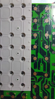
For example, the top side of the original PCB in the Canon P170-DH calculator uses what I think are carbon ink traces rather than copper. Likely this is because carbon traces can be used as contacts for the conductive pill keypad and left exposed to air without corroding. However, carbon ink traces have significantly higher resistance, which explains why the traces were made so wide.
One of the oddities of this board is that the power supply and printer driver components are mounted on the top of the board, while the calculator electronics are mounted on the bottom. Initially I thought this had to do with fitting into the three-dimensional space available in the shell, and so I did the same with the design of my replacement PCB. In reality there is at least 0.65 inches of space between the PCB and the shell, and the tallest component is barely 0.55 inches tall.
One morning this week, as I sat in traffic, a more likely explanation occurred to me. All of the components on the top of the board are through-hole parts, while all of the components on the bottom of the board are surface-mount parts. All the soldering is done on the bottom of the board, which I expect is required when using carbon ink traces on the top side.
All of the components I'm using are surface-mount, with the exception of a big filter capacitor and the connectors. If I was starting this design from scratch I'd give serious thought to putting all the components on the top, and the conductive-pad switch contacts on the bottom. Although KiCad has the ability to visually "flip" a board, it doesn't reorder the layers (yet!) which makes routing a bit more challenging.

Experiments with the world's first microprocessor
and other electronic explorations
Saturday, August 11, 2018
Tuesday, July 10, 2018
Demonstrating the SAP-1 Program Counter bug
Simulation is all fine and well, but the proof is comparing the results of the simulation with the real circuit. So I did just that.
Thursday, June 28, 2018
A structural version of the 74LS107A
Since I'd tested a structural simulation of the 74107 master/slave J/K flip-flop, I thought it appropriate to also test a structural simulation of the 74LS107A edge-triggered J/K flip-flop. The datasheet for the SN74LS107A from Texas Instruments provides a schematic for their chip, so I started there:


Monday, June 25, 2018
Last attempt with the M/S J-K Flip-Flop
With nominal gate delays added to all the TTL parts in my SAP-1 Verilog simulation, I decided to give the Master/Slave version of the 74107 J-K flip-flop one more try. And it flopped.
Sunday, June 24, 2018
A minor bug in the SAP-1 design
I put delays into the components used in the SAP-1 computer to better simulate the real chips. These delays are tiny compared to the 1 millisecond clock cycle of the SAP-1 -- generally on the order of 10 to 50 nanoseconds -- but they broke the simulated system: the RAM wasn't getting loaded with the correct values. I tracked this to the 9 ns propagation delay of the RAM address passing through the 74LS157 2:1 mux. A minor change in the timing generated in the testbench during these operations restored proper behavior.
BUT... while investigating this I discovered a bug in the SAP-1 design, and this one is not my fault.
BUT... while investigating this I discovered a bug in the SAP-1 design, and this one is not my fault.
Miswired adder... and the SAP-1 works
I found the "last" bug in my Verilog implementation of the SAP-1 computer. It looks like I did a cut-and-paste of the instantiation of the 74LS83 adder for the high-order 4 bits (C16) to create the instantiation of the adder for the low-order 4 bits (C17). I then connected the carry-in and carry-out signals correctly for both parts, but I forgot to change the bit numbers for C17. Thus the low-order bits weren't being driven.
Fixing this allows the SAP-1 to execute all 6 instructions of its program and produce the correct output on the emulated LEDs.
As satisfying as this is, it is not the purpose of recreating the SAP-1. The purpose is to help me understand more clearly how a computer fetches, decodes, and executes instructions.
Saturday, June 23, 2018
A bug in the SAP-1 Program Counter?
This morning I figured out what I did wrong with the SAP-1 Program Counter. But I think I also found a potential bug in the original design.
Friday, June 22, 2018
A good starter book
While browsing the web I came across some interesting references to a
 textbook called "Digital Computer Electronics" by Malvino and Brown. Originally published in 1977, and updated in 1983 and 1993, this book is out of print but still available on the used book market. One of the features is the step-by-step design of a simple computer the authors call the Simple As Possible computer, or SAP.
I've been tinkering with digital electronics since the Intel 8080 was new. I built a Science Fair project from TTL gates and circuits when I was in 9th grade (1976-ish). Thus the basics of digital electronics in general, and TTL circuitry in specific, are quite familiar to me. However, the opportunity to look at the instruction decoding and state transitions of a computer was quite appealing, and I hunted down a copy.
As is to be expected of a book last updated 25 years ago, the material is somewhat dated. The low-power Schottky TTL gates that were cutting edge then have been all but replaced by faster, more efficient CMOS technologies that this book notes in passing as low-power but very slow. That said, the design techniques are still valid. A NAND gate is still a NAND gate, even if the technology used to implement it is different.
Monday, June 11, 2018
Spice models
Every so often someone will ask for me to post the Spice models I've used (or tried to use). For some reason these requests usually get stuck in Blogger's spam quarantine, and I only notice them some weeks (sometimes months) later.
Rather than trying to keep up with these requests, I'm going to post links to these models here. Bear in mind that I didn't create these device models; I found them on the 'net. I offer no warranty on them.
Phillips (NXP) BSS83: BSS83_N.mod
Fairchild FDV301N: FDV301N.mod
Rather than trying to keep up with these requests, I'm going to post links to these models here. Bear in mind that I didn't create these device models; I found them on the 'net. I offer no warranty on them.
Phillips (NXP) BSS83: BSS83_N.mod
Fairchild FDV301N: FDV301N.mod
Eagle track length calculation errors
I decided to see if I could simulate the CLK1 and CLK2 signals on my current Instruction Pointer board using LTspice. Why these two? They're the only signals that have rapid rise times, as the others are all limited by the RC rise time curves of the pull-up resistors and the gate and drain capacitances they drive. To do this with any accuracy I needed to simulate the actual track lengths and capacitances at their ends.
Saturday, June 9, 2018
A clocking nightmare
Apparently I woo-hooed too quickly. I decided to run some simplistic simulations with LTspice to see what would happen with two boards connected to the output of a TC4427A. It wasn't good.
Thursday, June 7, 2018
Alarming clocks
An email from a reader pointed out that the 50th anniversary of the Intel 4004's commercial release in only three years away (Nov 2021). I think it'd be a fun idea to have my discrete component implementation of the 4004 running by then, so I may have to kick my efforts up a bit.
As I've said many times before, I'm a software engineer by profession and have no formal training in electrical engineering. So it's not surprising when design decisions I made five or six years ago turn out to be questionable in light of recently acquired understanding. In this case, I'm talking about transmission line behavior.
As I've said many times before, I'm a software engineer by profession and have no formal training in electrical engineering. So it's not surprising when design decisions I made five or six years ago turn out to be questionable in light of recently acquired understanding. In this case, I'm talking about transmission line behavior.
Tuesday, June 5, 2018
Terminator Two
Let's take another look at the termination of the transmission line for the CCLK signal. (And yes, I do like my puns.)
Ideally I'd use an IBIS simulator and the models provided by Xilinx for this purpose. Unfortunately I don't have access to one. The best I can do at the moment is some simulations with LTspice. Still, these are instructive.
Let's start with the circuit model. All of the simulations below were run with the same basic model, with some minor changes in connectivity and values as noted.
Saturday, June 2, 2018
The CCLK Terminator
There's a priority order when routing tracks on a printed circuit board. Highest on this list are high-speed circuits like clock lines where timing and waveform are critical. There are three such circuits on my P170-DH replacement PCB. One is the main system clock, which runs between a 50 MHz crystal oscillator and a global clock input on the FPGA. The second is the JTAG TCK line from the JTAG connector to the FPGA. The third is the SPI clock, known as "CCLK", between the FPGA and the Flash ROM. You might think that the 50 MHz system clock would be the most critical of the three, but you'd be wrong.
Friday, June 1, 2018
Contemplating worst-case scenarios
As I work on the replacement PCB for the Canon P170-DH calculator, I was reminded of a saying from a previous job: Design for Test.This means that you design a board with testing in mind, rather than trying to figure out how to test the thing after you've committed it to fibreglass, copper and silicon. Asking how I'm going to test this board led me to think about what might go wrong with it.
 My first concern is that I not end up with a smoking, fiery pyre on my work bench. This is one of the reasons I prototyped the FPGA +3V3 and +1V2 buck regulators, the +30V grid and anode boost regulator, and the filament driver.
Quite by accident, all the power circuitry ends up on the top of this board and all the logic circuitry goes on the bottom. Thus I can easily populate the top of the board and test the power subsystems before populating the logic components. After mounting the logic circuitry I'll recheck for short circuits before applying power, in case I get a solder bridge in a critical spot.
Hopefully this will keep the chances of smoking pyre to a minimum. What's the next worst thing that could happen?
Like all my hobby projects this one is a learning exercise, and even if it doesn't work completely at first I can still learn from my mistakes. I expect a single board to cost about $185, all told. If I find flaws in the design that I can't tolerate, a respin isn't out of the question. However, if the flaws are so bad that I have to respin the board just to be able to test things, possibly leading to yet another respin, that'd be painful. Aside from the smoking pyre, that's my worst case scenario.
My first concern is that I not end up with a smoking, fiery pyre on my work bench. This is one of the reasons I prototyped the FPGA +3V3 and +1V2 buck regulators, the +30V grid and anode boost regulator, and the filament driver. Quite by accident, all the power circuitry ends up on the top of this board and all the logic circuitry goes on the bottom. Thus I can easily populate the top of the board and test the power subsystems before populating the logic components. After mounting the logic circuitry I'll recheck for short circuits before applying power, in case I get a solder bridge in a critical spot.
Hopefully this will keep the chances of smoking pyre to a minimum. What's the next worst thing that could happen?
Like all my hobby projects this one is a learning exercise, and even if it doesn't work completely at first I can still learn from my mistakes. I expect a single board to cost about $185, all told. If I find flaws in the design that I can't tolerate, a respin isn't out of the question. However, if the flaws are so bad that I have to respin the board just to be able to test things, possibly leading to yet another respin, that'd be painful. Aside from the smoking pyre, that's my worst case scenario.
Thursday, May 10, 2018
I never learn
Once again I find myself contemplating using 0402 sized components. The 0603s just look so big compared to the FPGA pin spacing...
With the inner two layers under and near the FPGA taken by the +3.3V and Ground planes, and the top layer broken up by the keypad footprints and connecting matrix, I'm having to do a lot of routing on the bottom. The decoupling capacitors cover a lot of the periphery of the FPGA because they can't be mounted on top, so I think I'm going to use 0402s for the 0.47uF (high-frequency) capacitors that should be close to the chip. The 4.7uF (low-frequency) decoupling capacitors can be placed farther out, so they'll stay 0603s.
Watch this blog when I start assembling these boards for "Why do I do these things to myself?" type postings as I try to place these flakes of pepper on my board.
Wednesday, May 9, 2018
P170-DH Replacement Board layout progress
It may look like someone threw a handful of colored sticks on a black table, but this is the PC board that will go into my gutted Canon P170-DH calculator:

The mechanical outline, mounting holes, vacuum fluorescent display pads, and positions of the keypad contacts should be correct within a half-millimeter. The heavy gray lines that appear to partition the board are the locations of the support ribs on the bottom of the calculator shell that help support the PCB against the pounding of the keypad buttons.
The green square in the middle of the board is the Xilinx Spartan-6 LX9 FPGA; green pads mean it's on the back of the board. The 6x1 connector footprint at the top left is for the JTAG programming interface to the FPGA. The 20x2 connector is intended to allow me to plug my logic analyzer into the board through a ribbon cable; all free (and some semi-free) pins will be wired to this connector to maximize my debugging capabilities. The alternative would be the Xilinx ChipScope debugger which works through the JTAG, but I don't have the budget for that.
Clearly this isn't complete, given that there are parts that haven't been placed yet. Some circuitry hasn't even been added to the schematic, like the external serial interface. There's plenty of room for it, as long as I'm careful to avoid putting a via through a keypad footprint or a component under a support rib.
I figure I'm about a month away from sending this out for fabrication. When it's ready I'll probably use JLCPCB in China. I can get 5 boards from them for less than half the cost of one through US or European fabricators. If it was a matter of saving $5 or even $10, I'd buy locally (OSH Park does a great job), but when we're talking over $200 I'm going with the least expensive place with a good reputation.
BTW, this is all being done with the KiCad v5.0.0-rc2-dev pre-release. There are a few bugs still on the critical list, but it's remarkably stable. The v5 release fixes many of my biggest complaints about KiCad, and the developers are being very proactive about fixing problems as they learn of them. I've submitted about 25 bug reports thus far, most fairly minor (though one was graded a medium priority) and many were fixed within a day or two of being reported.
Tuesday, May 8, 2018
More info on the SST21x MOSFETs
When I searched for a MOSFET for use in my i4004 reconstruction, the only NMOS device I found that met my requirements was the Phillips (now NXP) BSS83. Production of the NXP BSS83 ceased in 2015.
In 2013 I found the SST211, SST213, or SST215 by CaLogic might be a suitable replacement, though the cost was significantly greater. Ouch.
When I search for the SST21x, I see four manufacturers: Siliconix, Vishay, Linear Systems, and CaLogic. Tonight I came across a press release from 2001 that explains some of my confusion over who makes these chips. It looks like the SST21x series was created by Siliconix. In 2001, Vishay, which by then owned over 80% of Siliconix, sold the the technology to manufacture the SST21x series to a company known as Linear Systems. So really the Siliconix, Vishay, and Linear Systems SST21x parts are the same. CaLogic claims their SST21x chips are a "proprietary design" so their FETs may be different but with nearly identical specs.
With the NXP BSS83 out of the picture, the SST211 or SST215 seems to be the best bet for a replacement. If you can afford to pay about $1/ea in 100+ quantity.
Saturday, April 28, 2018
FPGA Power test board
Here's the second of my power subsystem test boards being probed:

This one will supply 1.2V for the Xilinx Spartan 6 FPGA's logic core, and 3.3V for the FPGA's I/O interfaces and the 74LVC2G14 Schmitt trigger inverters. The VFD filament transformer driver will also run off this 3.3V supply.

This one will supply 1.2V for the Xilinx Spartan 6 FPGA's logic core, and 3.3V for the FPGA's I/O interfaces and the 74LVC2G14 Schmitt trigger inverters. The VFD filament transformer driver will also run off this 3.3V supply.
Friday, April 27, 2018
More iCEblink blues
I couldn't go to bed without trying the VFD power board with the actual vacuum fluorescent display. Which meant mating the iCEblink40 board with the VFD driver board. And once again I've run into problems.
VFD Power test board
Both the VFD power and FPGA power test boards showed up today. I decided to assemble one of them this evening, leaving the other for tomorrow.
Thursday, April 26, 2018
Understanding the V-t Product
I just realized I made an oopsie with my parts order from DigiKey. To understand why, we have to look at how transformers are characterized.
Wednesday, April 25, 2018
Gonna be a fun weekend
Why am I posting on a Wednesday afternoon? I got sent home from work because my allergies were making me sneeze so badly I really couldn't do much. Benadryl has calmed my sneezing, but writing this blog is about the most challenging thing I'm capable of at the moment. And that's questionable. :-)
On the bright side, this weekend is shaping up to be fun:
On the bright side, this weekend is shaping up to be fun:
- The parts I ordered from DigiKey early Monday morning arrives tomorrow via FedEx Ground.
- The VFD power subsystem test boards I ordered last Friday from OSH Park came back from the fab yesterday (Tuesday) and delivery is promised by 8pm Friday.
- The FPGA power subsystem test boards I ordered from OSH Park Monday just came back from the fab today (Wednesday). USPS says they'll arrive by 8pm Saturday.
Monday, April 23, 2018
Conductive Pad Keypad footprint
When you press a key on the Canon P170-DH keypad, it presses a conductive rubber "pill" against a pattern of exposed tracks on the PC board, shorting the tracks together. Here's a link to a good description of how this works. This is what that looks like on the original Canon PCB:
 This happens to be the largest of the patterns, under the most used key: the Plus ("+") key. It's about 8mm in diameter, while the smaller pattern is about 6mm. What looks like a single gold track meandering through the hole in the solder mask is actually the bare board between two tan-colored conductive carbon patterns. I don't know why they chose this odd pattern; perhaps it's for reliability, or has something to do with the way carbon tracks are constructed. For the longest time I had no idea what purpose the two exposed pads at 10 and 4 o'clock served, but I've come to believe these are test pads to allow testing of the carbon tracks and have nothing to do with the operation of the keypad.

Friday, April 20, 2018
FPGA Power circuitry
Earlier this week I finished the schematic for the FPGA power circuit using the LTC3607 dual buck regulator rather than the pair of TPS62170s as had been my plan. This evening I finished up the test board for this circuit and sent it off to OSH Park for fabrication. I expect to get it back before the first weekend in May.
Here's an image of the PCB, measuring 2" wide by 1.5" high:

Here's an image of the PCB, measuring 2" wide by 1.5" high:

Sunday, April 15, 2018
When is "Power Good" not good?
I've been putting together a couple of test PCBs to see how well my design for the power subsystems for the redesigned Canon P170-DH printing calculator. I figured it'd be smarter to build a couple of small (2" x 1.5") test PCBs at $15 each than to go all the way to the big (6.75" x 6.7") replacement board costing $150 and then discover that I'd made an error. In every case the circuit I started with is not the circuit I'm going to build.
Saturday, April 7, 2018
The resistance of a conductive pad keypad
I'm still relearning KiCad, so one of the first things I did while entering bits of schematic is the keypad. It's basically a 5 row, 8 column, matrix with a few contacts missing where there are larger keys.
 A resilient rubber sheet formed with bumps covers the PCB, each of the bumps under a key on the keypad. On the inside of each bump is a flexible conductive pad. Pressing the key pushes the conductive pad against a pair of bare conductors in close proximity on the PCB. These conductors meander in a pattern intended to maximize the area of contact, which minimizes the chance of missing a keypress.
Since these conductors are exposed to air, they must be corrosion-resistant. This board appears to use carbon rather than copper on the top of this board, which makes it quite resistant to corrosion. However, it also has a measurable amount of resistance to it. I believe the reason the traces visible in the photo here are so wide is to minimize that resistance.
This I knew from when I first disassembled and examined the board. I'd also measured the resistance of the conductive pad itself, which is quite low. What I'd never gotten around to measuring was how much resistance there was when the pad was pressed against the PCB, nor had I calculated acceptable values for the pull-up resistors on the rows and possibly columns. So tonight I made an attempt.
If you look closely at the photo (click on it to enlarge it) you'll find a key contact labeled "COST". Measuring from that to the via below the key contact area marked "GT" I see over 400 ohms. Measuring to the via above the "COST" key contact I see over 100 ohms. That's what I mean by "measurable resistance". Pressing the pad against the contact area gives a resistance of about 1.0K to 1.5K, depending on how hard the pad is pressed. If the carbon PCB traces account for 500 to 600 ohms I'd believe that the contact resistance accounts for the other 500 to 1K ohms.
I won't be making a PCB with a carbon layer on the top side, even if I knew where to get such a thing. On the other hand this is an experiment and I don't need that level of wear and corrosion resistance. My plan is to use normal copper with an ENIG (Electroless Nickel Immersion Gold) plating, which is easily available. This should give me reasonable corrosion protection while offering a flat surface. While I expect that will eliminate much of the contact resistance (and all but an insignificant amount of trace resistance), I'm still planning for 1K to 2K of resistance when a key is pressed.
Here's the schematic for the keypad as it stands now:

The 74LVC14 Schmitt trigger inverters I'm going to use to buffer these contacts wants to see a voltage below 0.7V before it considers an input to be low. The datasheet for the Spartan-6 family says the highest voltage on an output driven low is 0.4V, so the maximum voltage that I can allow to develop across the keypad contacts is 0.3V. If I hedge my bets and assume 2K through the keypad, Ohm's Law says 0.3V across a 2K resistor means there is 150µA flowing. Dropping the remaining 2.6V at 150µA requires my pull-up resistor to be 18K ohms or higher.
Looking at it the other way, an input of the 74LVC14 needs to reach as high as 2.0V before it sees the input as high. The datasheet says an input pin could leak as much as 5µA, so the upper limit on the pull-up resistor is 260K ohms.
There's also timing to consider. An input to the 74LVC14 presents a capacitance of only 5pF, but the contact patterns look a lot like tiny capacitors and the PCB traces are long. if I assume a bloated 50pF on each row, pulled up by a single 260K resistor, the RC time constant is 13µs. (In fact, it'll rise from 0.0V to 2.0V in 12.1µs, but who's counting?) This is far shorter than the 250µs I plan to assert the column output lines, so 260K would work.
As can be seen on the schematic, I'm planning to use 100K pull-up resistors on both rows and columns. This is the equivalent of one 50K ohm pull-up resistor when one switch contact is closed. There is also a 470 ohm resistor in series between the FPGA and the column of switch contacts.
Why the 470 ohm series resistors on the column drivers? My Verilog test code drives all the columns high, except for the one I want to probe which is driven low. If two switches on the same row are pressed at the same time, the low output of the column being probed and the high output of the other column are connected through the switches. That could damage the FPGA's driver circuitry. Digilent addressed this on their PmodKYPD keypad by placing 470 ohm resistors in series with the columns. If all seven keys in a row were pressed simultaneously, there would be seven 470 ohm resistors in parallel (equivalent to one 67 ohm resistor) in series with one 470 ohm resistor, for a total resistance of 537 ohms. With 3.3V across 537 ohms there would be a current of about 6mA. That's not ideal but it's insufficient to damage the FPGA.
Why the 100K ohm pull-ups on the columns? To avoid the issue of connecting two opposing drivers together, and thus avoiding the need for the series resistors, I could set the column drivers for the inactive columns to a high-impedance state. After all, the pull-up resistor on the row would pull the column high when a switch is pressed. However, digital logic really doesn't like inputs that float, and the columns that aren't being driven are essentially floating inputs. The column pull-ups keep these inactive columns in a known (high) state, as well as avoiding glitches on the rows when switches are pressed.
Laying out the PCB for both series resistors and pull-ups allows me to defer the decision on how to drive the columns until long after the board is fabricated. It's easy to leave the pull-up resistors off if I drive the columns high, and almost as easy to install 0-ohm "resistors" if I use the pull-ups. Or install both sets of resistors, which would permit either mode of scanning.
Isn't this fun?
Friday, April 6, 2018
KiCad display update rate fix
I've been working with KiCad to start the schematic and layout for the printed circuit board I'm going build to replace the factory PCB in the Canon P170-DH calculator.
The stable release of KiCad is 4.0.7, but I'm using bleeding-edge5.0.0-rc2-dev built from sources — literally last night's vintage. I don't recommend this for everyone (or anyone who isn't prepared for random failures and corruptions), but it seems to have reached a level of stability I'm willing to tolerate. I'm doing this largely because I have some modifications I'm developing, and I don't want to have to re-implement them when the 5.0 release comes out in a couple months.
The stable release of KiCad is 4.0.7, but I'm using bleeding-edge
Wednesday, April 4, 2018
The Need for Speed (and stability)
Monday I ordered some 10K 0.5% resistors in the 0402 package. As I ordered them I had the horrible thought that maybe, just maybe, they'd used 0201 packages instead, so I ordered a strip of those too.
Tuesday, April 3, 2018
M-32TL Printer contact debouncing
I got to thinking about the interface to the M-32TL printer from my Canon P170-DH calculator. Now that I have an async serial interface I thought I'd plumb it into the printer.
Sunday, April 1, 2018
More issues with the iCEblink40-HX1K
I decided it might be worth implementing a simple UART to allow the use of a PC serial port when testing the I/O peripheral interface. And it sounded like fun.
I looked on OpenCores to see if there was one I wanted to grab instead of writing my own, but most were complex clones of the 16550 UART chip, complete with a bus interface to control registers; far too complex for what I wanted. After all, the receiver is a simple state machine, and the transmitter almost trivial.
I coded up the transmitter in one evening. The receiver took a bit longer, about two evenings. Another evening was spent running it through the Xilinx iSIM simulator working out the kinks. I wrote a top module that took the output of the receiver and looped it back into the transmitter; something of a very complex loopback plug. I connected a PmodRS232 module to the board and connected that to one of my computer's serial ports. All that was left was loading it into the iCEblink40 board and giving it a test. I tapped a key... and got back garbage.
Sunday, March 25, 2018
Matrix keypad experiments, part 2
 Ever heard the saying, "The cobbler's children go barefoot"?
One of problems with being everybody's go-to guy for home tech problems is that there isn't anyone to call when your own tech develops problems. This morning I woke up to find my main computer and home network was completely locked up. Several frustrating hours later I finally got back to working on the keypad scanner.
The pic shows the iCEblink board with the PmodKYPD keypad plugged in, and my scope probes attached to the column 3 and 4 outputs.
Matrix keypad experiments, part 1
One of the tasks necessary to converting the Canon P170-DH calculator into a Busicom 141PF replica is to be able to scan the keypad. While I might have enough unused pins on the 144-pin Spartan-6 LX9 FPGA (max 102 I/Os) to connect each key to a pin, that's overkill for this requirement. Instead, I'll lay out the PCB to wire the keypad as a matrix.
Looking at the arrangement of keys, the obvious arrangement is 8 columns of 5 rows. This is different than the 8x4 arrangement of the 141PF, but then the two keypads don't have quite the same layout or keys:
Since making a PCB just to experiment with the keypad is more expensive than I'd like (about $150 US), I thought I'd start small, primarily with the resources at hand.
Looking at the arrangement of keys, the obvious arrangement is 8 columns of 5 rows. This is different than the 8x4 arrangement of the 141PF, but then the two keypads don't have quite the same layout or keys:
|
|

Programming the iCEblink40-HX1K from a Windows VM
Running Linux on your desktop brings with it some challenges. I found I'd installed a number of Lattice packages that might have been able to program the iCEblink, but I don't think I ever got any of them to work. I found a set of Digilent utilities (dadutil, djtagcfg) that will identify the board on the bus but I didn't see a way to program this board.
I found a project called iceBurn on GitHub that claims to be able to do it. This looks promising but I didn't feel like experimenting last night.
Eventually I remembered (or figured out again) how to do it from my VMware Player virtual machine running Windows 7. Here's the majick incantation for that:

Don't forget to flick the tip of your wand at the proper moment. Le-ve-OH-sa!
With this set-up I can run the synthesis, place & route, and generate bitmap files under Linux, then switch over to the Windows VM and program the board.
I found a project called iceBurn on GitHub that claims to be able to do it. This looks promising but I didn't feel like experimenting last night.
Eventually I remembered (or figured out again) how to do it from my VMware Player virtual machine running Windows 7. Here's the majick incantation for that:
- Configure the VM so it has a USB controller. This will allow the VM to claim a USB device on the host.
- Boot the Windows virtual machine.
- Install iCEcube2 2014.08. Later versions lack the programmer needed to program the iCEblink40. Be sure to install the programmer, which may be an installation option.
- Plug the iCEblink40 into the host using a USB-A to MiniUSB-B cable.
- Activate VMware Player's "Virtual Machine" menu and navigate through "Removable Devices" to the "Digilent Adept USB Device" menu. Click on "Connect (Disconnect from host)".

Don't forget to flick the tip of your wand at the proper moment. Le-ve-OH-sa!
With this set-up I can run the synthesis, place & route, and generate bitmap files under Linux, then switch over to the Windows VM and program the board.
Saturday, March 24, 2018
Using the Lattice iCEcube2 Software on Ubuntu 16.04
All you Windoze folk, go have coffee; this isn't for you.
Still here? Okay. This is mostly for me, so I don't have to figure this out anew every time I come back to this project.
Still here? Okay. This is mostly for me, so I don't have to figure this out anew every time I come back to this project.
Thursday, March 15, 2018
Tick... tick... tick...
One of my goals in designing a new PCB for the Canon P170-DH calculator is to add a key-click sound to positively indicate that a valid key-press has been detected. This was more important before I decided to implement the fluorescent display, but I think it's still valid.
Some people have done this by taking a piezo-electric transducer and driving it with a single, narrow pulse. Apparently this gives a sharp "TICK" sound. But I want something longer. And probably louder.
Some people have done this by taking a piezo-electric transducer and driving it with a single, narrow pulse. Apparently this gives a sharp "TICK" sound. But I want something longer. And probably louder.
Sunday, March 4, 2018
The more I think about it
The more I think about treating the rebuilt Canon P170-DH calculator purely as an I/O peripheral with a low-speed serial interface the more I like it. It would require far fewer signals than a parallel interface, while reducing the signal frequency from MHz to KHz. This reduces the risk level in completing the discrete-component i4004 CPU board set, which is far more critical now that the essential BSS83 transistor is no longer available. This will let me progress on the replacement PCB for the P170.
Saturday, February 24, 2018
External Interconnection issues
I've been trying to figure out how to interface the Canon P170-DH calculator I bought for its keyboard and printer and the discrete-component implementation of the Intel 4004 CPU. Long ago I decided to replace PC board in the P170 with one of my own design hosting an FPGA.
One of my design goals is that the rebuilt P170 should be able to operate either standalone with the i4004 CPU implemented in its FPGA, or using the discrete-component board stack as the CPU. As a standalone device the design is fairly straight-forward. To interface it to the external CPU it need some sort of external electrical interconnect.
It's resolving the nature of this interconnect that has been blocking my design of the new PC board for the P170.
Subscribe to:
Posts (Atom)