Thursday, July 26, 2012

Slow progress

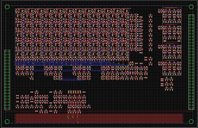
It's been a while since my last update. I've been busy with work, and haven't had much of a chance to focus on this project. However, I did get the rest of the circuit blocks routed, and I'm down to 50-some airwires.

The remaining tasks are:
  • Finish routing the connections between the circuit blocks.
  • Define the inter-board connector pin-out.
  • Route the inter-board connector.
  • Add some bypass capacitors between the VDD and GND planes
 After this, the board should be ready for fabrication. I've chosen PCB-Pool for fab, and the routing  complies with their design rule check requirements. One of the reasons for this choice is that they do an electrical test of all 4- and 6-layer boards they produce as part of the basic cost. Most other board houses either charge an extra $150+ for this, or don't offer the service. With about 600 discrete components on this board, most with at least one via to a power plane, the electrical test will save me hours of hair pulling.

I'm tired of posting screenshots that don't look any different that the previous picture. I considered posting that picture of a bunny with a pancake on his head, but it's been overdone. I just stumbled on a pic of the single bit DRAM cell on a breadboard, so I decided to post that:


This was when I was still trying to figure out how important the "bootstrap loads" were to the operation of the system. Rather than using lower-value passive resistors for this, I was considering using PNP transistors in a current mirror configuration; the three TO-92 components in the upper right of the breadboard are two active loads and the current reference. Also note that all the MOSFETs are BSS83s, as this predated my experiments with the FDV301s.

Monday, July 16, 2012

It Fits!

Not that it should be that much of a surprise, but I placed the remaining components and everything fits!


I haven't routed the newly-placed parts yet, but they shouldn't be much of a challenge. It's connecting the various groups together, and hooking stuff up to the connectors that may be interesting. Layer 16 (the bottom of the board) really doesn't have much on it yet, so if I'm careful with direction of route I should be able to get everything connected.

Sunday, July 15, 2012

Incrementer Carry

Real life has been keeping me from my hobby activities. Imagine that!

I did get the carry portion of the Incrementer placed and routed, though. It doesn't look like much, but here's the screen-shot:


Maybe I'll have time this evening to add the Row Select logic in that empty spot in the lower right.

Monday, July 9, 2012

Incrementer and Column Select

I'm glad I don't do PCB layout for a living -- this is real work! I'm finding I have to be in the right mood, or I end up staring at the components and see no way to route the connections. In the right mood, though, it takes just a few pokes and prods and then everything seems to work without effort.

You may have gotten the idea that I don't use the autorouter very much. I see lots of postings in discussion forums where people throw components on a board, click on "Auto Route", and expect everything to be done for them. Of course, the reason they're posting is the autorouter fails, or produces a tangled mess. I've occasionally given the autorouter a try, just to see what it'll do, but thus far I've never used the results.

This evening I got most of the Incrementer routed. To my surprise the original layout worked pretty well. Ok, I shouldn't be surprised: the real 4004 die and the schematic layouts are almost identical, and my initial layout is based on the same schematic. But I have some constraints the Intel folk didn't.

So here's the board at the end of this evening:


I still haven't placed the carry circuits, but that's next.

I placed the Column Select logic in the lower left of the board. This will drive the 3:1 muxes I placed earlier through the horizontal traces below the mux transistors. These traces appear blue in the screenshot because they're on the back side of the board. The Column Read Select circuits on the right edge of that group are routed, but I haven't started routing the Column Write Select circuits yet.

I also sketched in the group traces that form a sort of central bus in the 4004. The two external clock lines and all 8 of the phase enable lines are represented here. They appear as a hatched red in the screenshot because they're placed on layer 3, one of the two inner layers of the 4-layer board. My plan is to keep layer 2 as a solid ground plane (solid except for the thermals around the vias). When layers 1 (top) and 16 (bottom) aren't enough, I'll steal from the Vdd plane on layer 3.

I did a quick count, and there are 57 transistors and 21 resistors yet to be placed. Most of these are from the Row Select logic. I'm hoping that'll fit in the remaining area at the lower right of the board, otherwise I'll have to rearrange the Column Select logic to be higher and narrower. A quick count of layout grid squares says there is a 6 x 20 area free, but as with the Column Select logic, the structure doesn't necessarily lend itself to tight packing.

Friday, July 6, 2012

Incrementer placement

I had a couple of unexpected free hours last night, so I placed most of the "incrementer" circuit on the Instruction Pointer board. This circuit handles the normal incrementing of the instruction pointer from one instruction to the next, without requiring use of the ALU.

In this screenshot, the incremeter circuit is made up of the four groups below the DRAM array. I haven't routed them yet, so things may get rearranged a bit. The incrementer does its job in three 4-bit nibbles, presumably to save area. The group that handles the carry from one 4-bit nibble to the next hasn't been placed, but will live just to the right of the D0 group on the right.


Also visible are the Effective Address and Refresh counter groups along the far right edge. From top to bottom they are EA bit 0, EA bit 1, Refresh bit 0, and Refresh bit 1. If you click on the image to zoom in you'll see the footprints for the two capacitors I added below the EA bit 1 group in case this bit loses state too rapidly (see the previous posting for an explanation of the design flaw).

The best news is that I have about 73% of the components placed on this board, and what looks like plenty of space for the rest. I'm hoping to get the rest placed this weekend.

Thursday, July 5, 2012

Wherein the fundamental flaw is ultimately expressed

July 4th is a US national holiday, and amongst celebrating and catching up on my sleep I worked a bit on the Instruction Pointer board layout. I worked out a compact layout for the counters used to manage the refresh and effective address selection, and did the layout for all four bits. This brings the the IP board to 60% completion, as measured in placed and routed components, although this doesn't count the capacitors I added to the layout.

Which brings me to a flaw in the 4004's design.

Since the 4004 design is based on dynamic logic -- that is, it depends on storing a charge on the input capacitance of MOSFETs -- the state must be refreshed periodically or bad things happen. In most of the design this happens as a natural part of system operation. For example, the Instruction Register shown on Intel's block diagram really doesn't exist, it's just the charges stored on the inputs of the pairs of inverters that drive the decode logic. These "registers" are updated every time a new instruction is fetched, so they don't get corrupted due to charge leakage.

Other sections of the design must hold their values for extended periods of time, like the Instruction Pointer and Scratchpad Register arrays. These DRAM arrays have dedicated logic that makes sure they get refreshed periodically even if they aren't explicitly written by software.

One of the few "oopses" in the design is in the IP Effective Address counter. The first bit of this two-bit counter works just fine. Transmission gates T0371 and T0424 are driven by the CLK1 signal, so the charges on the gates of T0378 and T0420 are refreshed at least every 2 us. However, the same is not true for the second bit: when bit 0 is high transmission gates T0284 and T0353 are off, and will remain off as long as bit 0 remains high. The only reason bit 0 will go low is the execution of a subroutine call or return instruction. Thus, if the software doesn't execute one of these instructions for too long, the charges on the gates of T0294 and T0350 can leak away, changing the state of bit 1. This changes the row of the IP array used as the instruction pointer, causing the program to jump erratically.

I can't claim to have discovered this myself. I vaguely recall hearing that some microprocessor required occasional subroutine calls to work around a hardware defect, but that was decades ago and I don't recall knowing it was the 4004. Lajos Kintli pointed out this design flaw when I contacted him regarding my project. I'll have to ask him where he heard about it, just to avoid leaving that bit of trivia dangling.

With this flaw in the design in mind, it becomes a bit more clear why the test code the 4004 Analyzer runs by default starts by performing a sequence of three subroutine calls followed by three subroutine returns.

Since it's looking like I'll have board space to spare, I may lay out pads for capacitors between the gate and source of T0294 and T0350. My breadboard experiments suggest that the components I'm using will hold a "valid" charge for a shockingly long time -- several seconds, as I recall -- so I may not need these, but again it's easier to lay out pads now than to try to add them in later.

Sunday, July 1, 2012

Via in Pad?

I'm reminded of Bob Uecker's character Harry Doyle in "Major League", who makes a rude remark on the air. When challenged, he replies, "Nobody's listening anyway."

Just in case I'm wrong, does anyone have an opinion on placing a via inside a SMT pad on a board that's going to be hand-soldered? Most of the problems people caution about seem to be related to solder starvation, but I'm not worried about that.

Most of these vias would connect to inner layers (i.e. they go to VDD or GND), but I can create thermals on the inner layers as I don't need heat-sinking.

The Instruction Pointer Board

I'd always intended to implement the Instruction Pointer board first. It has an interesting mix of dynamic logic, NAND and NOR gates, and even four flip-flops forming two 2-bit counters. If I end up doing only one board, this is the one I want to do.

That it also has the most components makes it a good test for my area analysis too. If everything allocated to this board fits, the other boards will probably fit too.

I experimented with the layout of the DRAM cells for a while before settling on a 0.160" x 0.160" component placement grid, with each DRAM cell occupying a 2x2 square of the grid (0.320" x 0.320"). This puts the transistors close enough to minimize wasted space, while still allowing room for my tweezers and soldering iron. Or so I hope!

Each 2x2 square is laid out just like in the schematic, with the write enable gate in the lower left, the storage element in the lower right (the 3 pad package), and the read enable gate in the upper right. So what is the 2 pad package in the upper left of the square?

One of the great unknowns in this design is whether the input capacitance of the storage element FET will be high enough to hold the bit state through a full refresh interval. It works on my solderless breadboard, but I don't know whether that's because the breadboard adds parasitic capacitance. Rather than discovering that I need additional capacitance at that point and having to trash the board, I've added a footprint for a discrete capacitor in the fourth grid square. If the circuit has sufficient margins without it I'll leave that space unpopulated, but if needed I'll have a place to put it.

Yesterday I started the layout of this board for real. I got the entire 12x4 array of DRAM cells placed and routed, along with the output precharge FETs across the top and the output inverters along the bottom. I also placed the 3:1 muxes below that and the row decode components along the right edge of the array, but they're not routed.

Here's a snapshot of the board thus far (click to expand):


I've placed all but a handful of the 248 components from Sheet 1, which puts me at about the half-way point with more than half of the board area remaining. There should be enough room to place and route the rest of the components I've assigned to this board, but I'm a bit worried that I'll be forced to place the random logic on a larger grid to get it routed. Worst case, the components on Sheet 4 or 5 could be moved to the timing board, but that would bode poorly for the rest of my area analysis.

My hope is that everything will fit nicely enough that I can go ahead and build this board without doing the layout for the others first, but if things get really tight I might feel the need to finish all the layout first. And that might start feeling like real work.

Interconnection


One of the regional cliché phrases is that of a New Englander responding to a request for directions with, "You can't get there from here." Usually pronounced as "Ya cay-ent git they-uh from he-uh." Ok, it's funny to me.

One of the things that I find most challenging is mechanical interfaces. The sheer number of connectors and mechanisms just feels overwhelming. How to choose?

I started off thinking of the classic card-edge connectors and some sort of backplane. I gave serious consideration to the STD bus until my partitioning analysis showed that its 56-pin capacity wasn't nearly enough: the current partitioning requires 72 pins, including power and ground, and I want a bunch of free pins in case I need to repartition late in the process. I put the issue aside for a while.

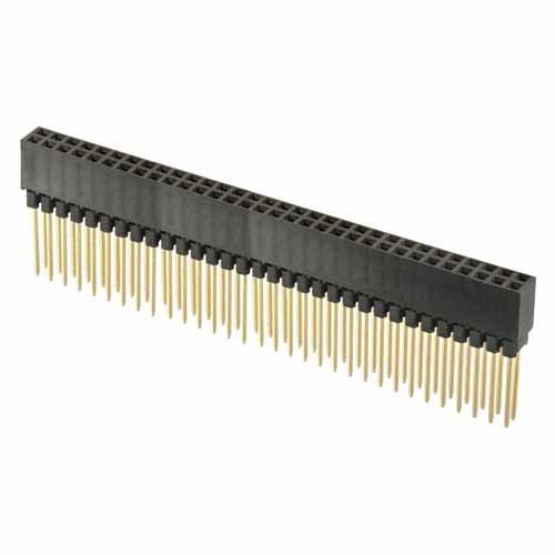
While cleaning up files from old projects I came across one that used a PC/104 board stack. PC/104 is an embedded computer form factor where various boards plug directly into each other without using a separate backplane. A PC/104 connector is mounted with the socket on the component side of the PCB. The pins of a "stackthrough" connector are long enough to go through the PCB and plug into the socket on the board behind it.

Here's a drawing from the PC/104 Consortium website showing how the boards stack:

The original PC/104 spec implemented the old 8-bit ISA interface on a 64-pin connector. This was later extended to support the 16-bit ISA interface by adding a 40-pin connector, giving a total of 104 pins.

Although I have no intention of using the PC/104 card dimensions or connector pinouts, the connectors themselves are ideal for my purposes. Since all signals show up on all connectors the boards can be assembled in any order, giving easy access to whichever board is on top. Since I need more than 64 pins I'm putting a connector at each end of the board. My current drawings have a 64-pin connector on the right end and a 40-pin connector on the left, but I could easily put 64-pin connectors at each end for a total of 128 inter-board connections.

Here's a snapshot of the board layout as shown in the Eagle package editor, showing the connectors at the left and right ends of the board:


The dimensions at the left and bottom show the board dimensions: 6.6" x 4.25". This is somewhat larger than the maximum component area supported by my Eagle Standard license, depicted here by the dot-dash border line. Eagle's limit applies to component pins and pads, though, and not to signal traces; I can place components smack up against the legal area and still be able to route traces to them from any side. Thus I've made the board a little bit larger to be able to do that.

Partitioning

Since I can't, and don't want to, create one single board, the next task was partitioning the design into manageable pieces. Here's the partitioning as depicted in one of Intel's own datasheets:


Each of the two DRAM arrays, the Instruction Pointer and the Scratch Pad, form distinct blocks. This is also clear from looking at the schematic in my previous posting: the Instruction Pointer is the upper left group, the Scratch Pad the upper right group. Other blocks of significant complexity include the Instruction Decoder and the Arithmetic Logic Unit.

As you can imagine, dealing with a single schematic sheet taller than I am would be unwieldy. Also, to be able to lay out separate boards the schematic needed to be broken into one or more sheets per board. After partitioning, the sheets making up each board can be copied to a new schematic and the board laid out from that.

I settled on ANSI "D" size (22" x 32", or about ISO A1) for my schematic sheets. This avoided having to break most of the big blocks into pieces, the Instruction Decoder being the exception. With a 2:1 reduction, this prints nicely on an ANSI "B" sheet (11" x 17", roughly ISO A3), a commonly available size that fits through my color inkjet printer. At this size the text is a bit hard to read, but the structure is easy to follow.

I wrote an Eagle User Language Program (ULP) to print a report of component counts on each sheet. By tagging each sheet with a board assignment label, the ULP also reports the component totals for each board. I wanted to minimize the number of boards, while maintaining the functional groupings. Another ULP that reports the inter-board connections helped guide the partitioning.

Here's the current partitioning, by sheet and by board:

Sheet  1:  Ts: 226  Rs:  18  Bs:   4  Total:  248  Instruction Pointer DRAM Array
Sheet  2:  Ts:  55  Rs:  13  Bs:   0  Total:   68  IP Incrementer
Sheet  3:  Ts:  40  Rs:  16  Bs:   0  Total:   56  IP Row & Refresh Counters
Sheet  4:  Ts:  44  Rs:  15  Bs:   0  Total:   59  IP Column Decode Logic
Sheet  5:  Ts:  53  Rs:  18  Bs:   3  Total:   74  IP Selection Logic
Sheet  6:  Ts: 272  Rs:  20  Bs:   8  Total:  300  ScratchPad DRAM Array
Sheet  7:  Ts:  75  Rs:  19  Bs:   0  Total:   94  ScratchPad Decode & Refresh
Sheet  8:  Ts:  77  Rs:  24  Bs:   5  Total:  106  ScratchPad Selection Logic
Sheet  9:  Ts: 203  Rs:  45  Bs:   2  Total:  250  Instruction Decode 1
Sheet 10:  Ts: 134  Rs:  34  Bs:   1  Total:  169  Instruction Decode 2
Sheet 11:  Ts:  46  Rs:  19  Bs:   2  Total:   67  Instruction Decode 3
Sheet 12:  Ts: 234  Rs:  52  Bs:  15  Total:  301  Arithmetic Logic Unit
Sheet 13:  Ts: 110  Rs:  32  Bs:   5  Total:  147  Chip Select Logic
Sheet 14:  Ts:  81  Rs:  15  Bs:  12  Total:  108  Clock & Timing Generation
Sheet 15:  Ts:  99  Rs:  21  Bs:   9  Total:  129  I/O Buffers - D0..D3

Boards:
 Instruction Pointer:  Ts: 418  Rs:  80  Bs:   7  Total:  505
         Scratch Pad:  Ts: 424  Rs:  63  Bs:  13  Total:  500
  Instruction Decode:  Ts: 383  Rs:  98  Bs:   5  Total:  486
                 ALU:  Ts: 344  Rs:  84  Bs:  20  Total:  448
        Timing & I/O:  Ts: 180  Rs:  36  Bs:  21  Total:  237


As you can see, I have five boards planned. The first four contain the majority of the circuitry, with the fifth board left as a sort of "catch-all" for what doesn't fit on the others. My rough area analysis suggests this will work, but as a novice creating such complex boards I'm allowing for the possibility that I could be wrong. There's room on the "Timing and I/O" board for some overflow, and the inter-board connectors have plenty of unused pins.