- CLK1 == 1'b1
- D[0:3] == 4'b1111
- M12+M22+CLK1~(M11+M12) == 1'b1

Experiments with the world's first microprocessor
and other electronic explorations
Wednesday, December 30, 2015
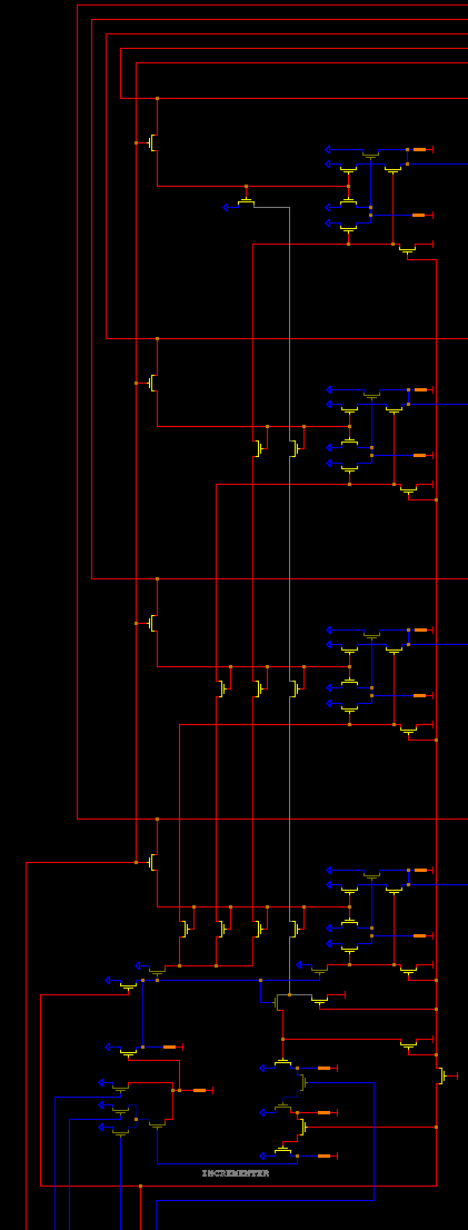
Incrementer shoot-through analysis
The problem I'm investigating occurs when the incrementer circuit attempts to pull a signal high and low at the same time. This happens whenever these conditions are all true:
Tuesday, December 29, 2015
Shooting the Incrementer
The next oddity I though I'd investigate is the always-on pass transistor in the CLK1 signal in the IP incrementer. You can spot it on the far right edge and near the bottom of the picture below; look for the FET with its gate hard-wired to Vdd.
 When I built my IP board I blindly followed the i4004 design, and the incrementer seemed to work during my testing described in my post Like a Phoenix back in September 2012. But this FET has always been a source of confusion. Why would the chip designers do this?
I dreamed up various theories. The one that seemed most likely was a critical timing condition, as a signal passing through such a FET would incur some small delay. Another thought was some sort of ringing in the chip, with this FET acting as a snubber. I thought about putting my IP board on the bench and see what effect this FET might have, but I'd be probing blindly.
So what function does this signal (N0325 in the simulator) perform? It seems to cause some signals to be driven high that may or may not be pulled to ground later, a common dynamic logic technique used in the DRAM array and elsewhere. But while stepping the simulator through the first carry operation (00F to 010) I noticed something strange: some of the signals go into "undefined" states (circuits colored gray in the picture). This means that they're being driven both high and low at the same time. This can result in "shoot-through", where Vdd is connected to Vss through a low-resistance path. Ouch!
This seems to be the case in the screen capture I posted above. This particular capture occurred at cycle 1586 but it's not a unique situation. Yet I can't imagine Intel could meet power dissipation targets with large shoot-through currents. So what's going on?
Maybe there isn't a low-resistance path. That might happen if the FET driving the signal high isn't turned on fully. How would you keep this FET from turning on fully? You'd lower the gate voltage. That pass transistor might have that effect; the output voltage would be limited to a maximum of Vdd - Vgs. Remember that CLK1 (and CLK2) are driven externally much closer to Vdd than other inputs. Unfortunately I really don't know the gate threshold voltage of the P-channel MOSFETs used in the real i4004.
Wouldn't I have seen signals going into undefined states in my testing? The Verilog version of the incrementer is behavioral, not gate-level, so it wouldn't have shown up there. It's not a situation I considered when testing the actual IP board, and my logic analyzer's buffer limitations prevented me from seeing the carry out of the first nibble to the second. I can't even say for sure that the nibble-carry works.
Once again, I seem to have a mystery on my hands. I'll have to put my IP board on the bench and see whether the incrementer handles carries from one nibble to the next properly. I'd like to probe the circuits that go to "undefined" states with my oscilloscope, but I'll have to give some thought to how to trigger on it.
Sunday, November 8, 2015
The Bootstrap Load mystery solved
Sunday, October 25, 2015
Deeper into the mystery
Continuing from the previous post, I zoomed in so each horizontal division represents a mere 5ns rather 500ns, and triggered on the falling edge of row read enable. It's not at all clear to me what is going on, so if you see problems with the following analysis PLEASE let me know!
Friday, October 23, 2015
Everyone loves a mystery
Everyone except engineers, that is. Mysteries without solutions lead to Unexpected Results and we don't like those. Not one little bit. So I went back to the DRAM cell tests I performed in June 2012 to solve the mystery of why the FDV301 wouldn't work as the read-enable transistor.
Tuesday, October 20, 2015
My first DMCA Takedown notice
No, no one is asking me to take down this blog or my OpenCores project. Instead, someone "scraped" the OpenCores site and pulled all the various projects into a single repository hosted on GitHub.
Saturday, October 17, 2015
Margin testing detail
Here's a schematic of the worst-case margin test circuit:
 In all cases the substrate pins are pulled to ground. Here's a brief overview of the circuit:
My first series of tests were performed with the circuit as shown. Here's a table of the results:
At VDD of 3.0V, the Q5 Vs (which is also the Q6 Vg) was below the level sufficient to turn on Q6. This is the failure criteria.
My second series of tests were performed with two modifications to this circuit: Q3 was replaced with a DMN26D0UT and Q4 was replaced with an FDV301. Here's a table of the results:
At VDD of 3.0V, the Q5 Vs was just high enough to turn on Q6, albeit slowly; a very small VDD decrease resulted in failure. It's pretty clear that using a DMN26 for the high-side driver boosts the push-pull "high" output by about 0.7V, which translates to similar increase in a pass-through voltage.

- CLK1 and CLK2 are two non-overlapping, positive-going, pulses. I used a PIC to generate the two clocks.
- Q1/R1 serve to isolate the output of the PIC from the varying VDD of the test circuit. It also converts the PIC's push-pull output to something more characteristic of the signals generated by the resistive pull-up design of the i4004.
- Q2/R2, Q3, and Q4 form the push-pull output circuit commonly used in the i4004 to drive high-capacitance circuits. R2 would normally be "bootstrap load".
- Q5 is used as a "transmission gate" or "pass gate". This is the one situation where a four-terminal MOSFET like the BSS83 is critical, as the substrate must be kept at a lower voltage than the channel or the body diode will conduct. The input to Q5 would normally be a logic signal, but for this test it's strapped high.
- Q6/R3 form a simple inverter to allow measurement of the threshold voltage of a BSS83 in grounded-source mode.
- Q7 discharges the gate of Q6 to allow observation of the turn-on characteristics of Q5.
- With CLK1 low Q1 is off, allowing R1 to turn on Q2 and Q4; Q2 thus turns off Q3. With Q3 off and Q4 on, the gate of Q5 is pulled to ground, closing the transmission gate and preventing input changes from affecting Q6. Q6's gate floats, holding whatever value it previously had.
- When CLK1 goes high, Q1 turns on. This turns off Q2 and Q4; R2 thus turns on Q3. With Q3 on and Q4 off, the gate of Q5 is pulled to VDD less the Vgs(th) drop across Q3. The input signal to Q5 (VDD, in this case) is passed to the gate of Q6; if this level is sufficient to turn on Q6, OUT will go low.
- When CLK1 goes low again, Q5 will turn off. The capacitance of the gate of Q6 and the circuit driving it will hold whatever level was present on the input of Q5.
- When CLK2 goes high it turns on Q7, discharging the gate circuit of Q6 and causing OUT to go high.
My first series of tests were performed with the circuit as shown. Here's a table of the results:
| VDD | Q5 Vg | Q5 Vs | Q5 Vgs |
| 7.0V | 5.6V | 4.2V | 1.39V |
| 6.0V | 4.6V | 3.3V | 1.33V |
| 5.0V | 3.7V | 2.4V | 1.30V |
| 4.0V | 2.7V | 1.6V | 1.19V |
| 3.5V | 2.5V | 1.4V | 1.17V |
At VDD of 3.0V, the Q5 Vs (which is also the Q6 Vg) was below the level sufficient to turn on Q6. This is the failure criteria.
My second series of tests were performed with two modifications to this circuit: Q3 was replaced with a DMN26D0UT and Q4 was replaced with an FDV301. Here's a table of the results:
| VDD | Q5 Vg | Q5 Vs | Q5 Vgs |
| 7.0V | 6.4V | 4.9V | 1.48V |
| 6.0V | 5.4V | 4.0V | 1.44V |
| 5.0V | 4.4V | 3.1V | 1.33V |
| 4.0V | 3.4V | 2.1V | 1.26V |
| 3.5V | 2.9V | 1.65V | 1.24V |
| 3.0V | 2.4V | 1.25V | 1.21V |
At VDD of 3.0V, the Q5 Vs was just high enough to turn on Q6, albeit slowly; a very small VDD decrease resulted in failure. It's pretty clear that using a DMN26 for the high-side driver boosts the push-pull "high" output by about 0.7V, which translates to similar increase in a pass-through voltage.
Friday, October 16, 2015
Margin Testing
Now that I understand the function and operation of the "bootstrap load" circuit, I thought I should go back and reevaluate my assumptions and implementation.
Analysis suggests, and experimentation confirms, bootstrap loads have little to do with signal rise-time and everything to do with voltage margins. I had been expecting to see them used when the capacitive load was high, but these are driven by push-pull "totem pole" circuits. Instead they're used to pull up the gates of pass transistors, or to pull up the gates of the high-side push-pull drivers that drive pass transistors. I could probably replace all of them with the same 4.7K resistors I used for the normal loads.
This triggered a bit of anxiety: I know my IP board works, but how close is it to failing? Is it just barely working, or is there margin for component variation? In this, the BSS83 gave me the most cause to worry. Its gate threshold voltage is unhelpfully specified as being "greater than 0.1 and less than 2.0 volts". The thing is, I have no real choice but to use it for the pass transistors; every other choice is either crazy expensive or has gate capacitances of several hundred picofarads.
Since I couldn't get to my lab until late this evening I gave some thought to alternative solutions, if there were a problem. One was to raise Vdd above 5V, which had been chosen somewhat arbitrarily. The limiting factor here is the FDV301, which has an absolute maximum Vgs of 8V, followed by the BSS83's max Vds of 10V. I expect the only negative effect of raising Vdd to 6V or even 7V would be increased power consumption. If that were the only cost of making the design work, it'd be worth it.
Once I got to my lab, though, I was able to measure actual voltage margins under controlled conditions on my breadboard. The randomly-chosen BSS83s I tested in a pass transistor configuration limit the passed voltage in either direction to 1.33V less than the gate voltage. The worst-case scenario is a BSS83 pass transistor, whose gate is being driven by a BSS83 high-side push-pull driver (Vdd - 1.3V), and whose output is driving a BSS83 in a common-source inverter configuration. In this configuration, the noise margin is significantly reduced. Since signals are gated onto and off the data bus through sequential pass transistors I worried that this effect would be cumulative, but it isn't.
With a handle on the situation I finally ran the margin tests on my breadboard, as I said I was going to do three years ago. The worst-case circuit fails with Vdd below 3.5V (the inverter doesn't turn on). Between 3.5V and 4.0V the circuit runs with increased propagation latencies and slow signal transitions compared to 5V operation. Above 4.0V and up to 7.0V (the highest I tested) the circuit is stable, with a very small reduction in latencies up to about 6V. Replacing the high-side driver with an FDV301, as described in the post Unexpected results, or a DMN26 reduces the high-side driver loss to 0.6V, which improves the margins such that it will just barely operate at 3.0V. This gives me confidence that the entire circuit should work at 5.0V, though I will make sure I don't do anything to prevent raising Vdd to 6V if need be.
There's one more step I may take as I work toward completing this project. In the intervening three years I have hand-assembled several dozen boards using 0402 (0.50 x 1.00 mm) passives. After that the DMN26D0UT in its SOT-523 (0.80 x 1.60 mm, about 0603) packaging no longer scares me. I'm seriously considering using it to replace the BSS83 as the high-side driver in the tristate output circuits, where the FDV301 can't be used because of its gate-to-source protection diode. Its lower Vgs[th] would increase the output-high voltage by almost a half a volt.
Tuesday, October 13, 2015
Puzzling out the Bootstrap Load
One of the sub-circuits in the 4004 that has always confused me was the so-called "bootstrap load". It's depicted in the schematic as a resistor with a "B" next to it, but the legend gives more detail. Remember here that I'm a software engineer and have no formal training in electrical engineering, let alone materials science.
Researching the construction of integrated circuits reveals that true passive resistors can take up a significant amount of silicon area, while transistors are usually smaller. By careful design of the transistor, it's possible to create a small transistor that acts pretty much like a passive resistor. Thus the legend indicates that what is shown on the schematic as a pull-up (or "load") resistor is really a single MOSFET with its gate and drain connected to VDD.
However, the "bootstrap load" circuit shown at the bottom is more complicated. It consists of two MOSFETs and a capacitor. How does this thing work? I made the assumption that bootstrap load was used when a faster rise-time was needed, but I really didn't understand how this circuit worked.
 |
| i4004 Schematic Legend |
However, the "bootstrap load" circuit shown at the bottom is more complicated. It consists of two MOSFETs and a capacitor. How does this thing work? I made the assumption that bootstrap load was used when a faster rise-time was needed, but I really didn't understand how this circuit worked.
Subscribe to:
Comments (Atom)