
 Here's the test circuit. This is a extract of the real 4004 schematic,
and the names are taken from the 4004 simulator. The three signals
driven by the PIC are labeled on the right edge.
Here's the test circuit. This is a extract of the real 4004 schematic,
and the names are taken from the 4004 simulator. The three signals
driven by the PIC are labeled on the right edge.The top most signal with the hideous name of
The middle signal, named N0444 here, is the row read enable. It goes active to gate the drain of the storage element T1268 to the column sense line through T1280. This signal is shown on the 'scope traces in yellow.
The lower signal, named N0439 here, is the row write enable. It goes active to charge the gate of the storage element T1268 to its new value.
The problem I'd encountered when testing an FDV301 as T1280 was the column sense line would go low as the row read line went low, even when it should have remained high. Since we're mostly interested in the behavior of T1280, I've placed my other two 'scope probes on the column sense line N0770, shown in blue, and on the source of T1280, signal N0834, shown in magenta. To ensure the storage element T1268 remains off, I removed the write enable gate T0240 and pulled the gate of T1268 to ground through a 1K0 resistor.
The four oscilloscope probe inputs are shown in the upper half of these screen shots. All of these share the same units and ground level, 2V/division with ground level one division above center. To make things even more clear, I've done some magic with the oscilloscope so T1280's apparent Vds is displayed in light green, and its apparent Vgs is displayed in orange. These two traces are shown in the lower half of the screen, again with 2V/division but with ground level two divisions below center.
First we'll look at the behavior of the circuit as implemented in my IP board, with a BSS83 as T1280. Recall that the BSS83 is a four-terminal device, and the substrate is connected to ground.
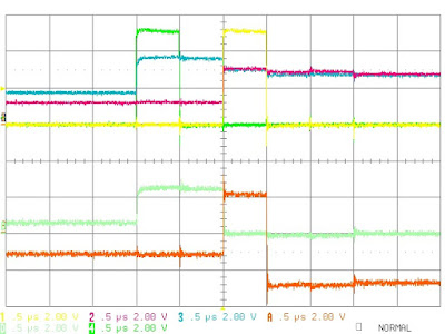
This is a working circuit, so let's figure out what it's showing. First look at the upper half of the display. When column pre-charge enable goes active column sense is charged to 3.6V, where it remains due to the various capacitances in the circuit. When read enable goes active T1280 turns on, which causes some of the charge on column sense to be transfered to N0834.
The lower half traces make things even clearer. When column pre-charge enable goes active, Vds rises from about 0.4V to 2.4V. Then when row read enable goes active, Vgs goes from -1.0V to +2.2V, turning on T1280 and causing Vds to drop to 0V. When row read enable goes inactive Vgs goes to -2.8V, turning off T1280 with little change in Vds.
Whew!
Now let's look at the same circuit with a DMN26D0UT as T1280. This three-terminal MOSFET has the substrate connected to the source, and back-to-back 10V Zener diodes between the gate and the source.

These results are similar to those with the BSS83. When row read enable goes active both N0834 (the source) and Column sense (the drain) go a little higher, perhaps reflecting the lower turn-on threshold voltage of the DMN26. When row read enable goes inactive N0834 (the source) goes a little lower, resulting in a higher Vds of about 1V. Since the source is a bit lower wrt ground Vgs goes only to -2.0V, which is insufficient to turn on the Zener protection diodes.
Now let's take a look at the FDV301 as T1280. This three-terminal MOSFET has the substrate connected to the source, and a simple diode between the gate and the source.

Things aren't too bad until row read enable goes inactive. When this happens the gate-source protection diode is forward-biased and conducts, pulling e N0834 (the source) to a diode-drop above ground. As this happens it pulls column sense to ground too. This demostrates the failure mode I saw in 2012.
It'd be interesting to zoom in much more closely on the period where row read enable goes inactive and see if I can see evidence that the FDV301 remained turned on, or if this is a charge-transfer effect.
What really surprised me was that this circuit seems to work with the DMN26, which is contrary to my 2012 results. I suspect this is because I'm driving the enable circuits directly from the PIC, which drives all the way to +5.0V, while my 2012 test recreated much more of the 4004's circuitry on the breadboard.
No comments:
Post a Comment