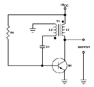
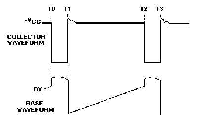
I often start with Wikipedia, but in this case the wiki article is terrible. It goes into great detail without first giving a basic overview of the circuit operation. Looking elsewhere I found a pretty decent description on the Integrated Publishing website starting here. The good stuff start several pages in from the link above, but I'll summarize it. Clicking on the schematic or idealized waveform drawings will take you directly to the source web pages.
 |
| Blocking Oscillator circuit diagram |
 |
| Blocking Oscillator idealized waveforms |
It's interesting to compare the idealized waveforms to this one from the calculator. The yellow (bottom) trace is the transistor collector waveform, and the red trace above it is the transistor base. These are quite close to the idealized waveforms.
In the calculator circuit Vcc is normally around 9VDC, though for my tests I'm keeping it at 7.25 volts for reasons I'll explain later. R1 is 1,500 ohms and C1 is 4.7 nF (0.0047 μF, if you prefer). There is also a 100 ohm resistor between L2 and C1 that isn't shown in the schematic above; the green trace at the top of the scope screenshot is the L2 side of this resistor and the blue trace is the C1 side. I've also done some 'scope magic to display the voltage drop across this 100 ohm resistor (the pinkish trace), thus showing the current through the resistor on a scale of 20 mA per division. It's a bit hard to see on the screenshot, but I'm seeing a peak of +25 mA when the transistor starts to conduct and -40 mA when the transistor turns off. That's more than enough to overwhelm the basic bias current through R1 of 4.5 to 6 mA.
This is not the entirety of the power circuit, though. If the AC mains voltage is high enough to drive the unregulated Vcc voltage above about 7.7 volts another circuit grounds the base of Q1 for periods, causing the blocking oscillator to run in bursts. This appears to be a form of PWM voltage regulation to limit the output from the transformer. I haven't finished analyzing this part of the circuit enough to describe it further.


No comments:
Post a Comment