Monday, December 19, 2016

More on the M-32TL printer

The last couple of weekends I've stolen a few hours here and there to put my logic analyzer on the M-32TL printer in the Canon P170-DH calculator I've chosen as a keyboard and printer interface to my 4004 CPU reconstruction.


Here you can see the USB logic analyzer pod on the left, and the under side of the calculator on the right. The printer is visible in the upper right corner.

This printer can print in either black (blue-ish, anyway) or red. I previously linked to a web page by Arne Rossius with his analysis of the similar M-31A printer, but of course it gave no hints as to how the shift to red worked. By recording the signals received from the position sensor and the signals driving the motor and solenoid, I've been able to get a better idea how this printer works.

Although I found the pinout to be the same as described in the M-31A, I disagree with Arne's description of the function of the position sensor signals.

PinFunction
1Solenoid -
2Solenoid +
3Motor +
4Motor -
5Solenoid index
6Rotation index
7Sensor common
8Character index

In the P170-DH, pins 2 (Solenoid +) and 3 (Motor +) are connected to the unregulated positive supply, which seems to provide a bit under 8 VDC. Pin 7 (Sensor common) is connected to ground, while pins 5, 6, and 8 are pulled to a logic "high" through resistors and debounced with an RC network. When a sensor contact connects with the conductive pattern etched on the sensor disc it pulls the logic input low.

Here's where my analysis differs: When pin 8 goes low, the printer wheels are approaching the next character. If pin 6 is also low it's the first character in the sequence given below, else it's the next one in the sequence. If this character is to be printed the solenoid is activated when pin 5 next goes low and remains activated until pin 5 goes low again.

Why not just use pin 5 to determine the character position? It appears from the signal recordings that while the character is being printed the wheels stop moving briefly. During this time pin 5 often generates several erratic low indications, while pin 8 never does. I suspect the contact for pin 5 is just on the edge of the conductor pattern on the sensor disc and any movement of the disc causes the contact to make and break. This would result in printing errors.

It also appears that this printer can print from the "Symbols" wheel in the right-most two columns, rather than only one. I haven't seen this calculator do it yet, but the second character printed thus far has always been index 10, which is a space. There's definitely enough of a gap between the right most symbol and the first number for one if not two more characters.

Wheel Character Printed
Symbols + × ÷ Δ G M C = (space) % (red)
Numbers 0 1 2 3 4 5 6 7 8 9 , #

The third character appears to be the key to the color shift. If the number portion is to be printed in black, the third character is index 10 (a space). But if the number is to be printed in red, the third character is index 13; this also prints as a space, but all following characters are printed using the red number wheel.

Printing of a line is completed by activating the solenoid for much longer than a single character time while printing the final character. In my tests the P170-DH asserted the solenoid for just under 24ms.

At some point I'll want to disconnect this printer from the calculator board so I can test it with a PIC as a driver. The reason I haven't done so yet is I'm not sure I've learned all I can before I start disassembling it. I do have a second P170-DH, but I'd rather not have to open that one up unless I need to.

Sunday, November 27, 2016

Tweaking the FDV301N Spice model: Cgs

To improve my Spice model of the FDV301N MOSFET I need to understand a little more about how they work. A lot of the dynamic behavior can be modeled as three capacitors: Cgs, Cgd, and Cds. The complexity, as seen in the model provided by Fairchild (diagrammed in the previous post), comes from the fact that the value of Cgd changes as Vgd changes. This post focuses on measuring and modeling the simplest of these: Cgs, the capacitor between the Gate and the Source.

To make life more fun, the data sheet doesn't give the value of Cgs. They give three other values, Ciss, Coss, and Crss:


My research says that Cgs can be calculated as Cgs = Ciss - Crss, so Cgs for the FDV301N should be 8.2pF. The updated Spice model Fairchild provides models Cgs as 8.5pF, which seems close enough. But how do you compare this against the real device?

As a MOSFET is driven on with a constant-current source, its gate voltage does not rise linearly. As the drawing on the right (from ON Semiconductor publication AND9083/D) shows, Vgs behavior can be characterized in three phases. In phase A (red), the gate current is charging Cgs, but Vds has not begun changing. In phase B (blue), the transistor begins to conduct and Vds begins to drop, which means the voltage across Cgd is also changing. With the gate current being consumed charging Cgd, Vgs does not change. In phase C (green), Vds has reached its minimum (or near enough to it) and the gate current goes toward charging both Cgd and Cgs.

Long ago I created an LTspice model of a chain of FDV301N inverters for simulation testing. To this I added 10pF capacitors between the gates and ground to represent my oscilloscope probes. I also replaced the U2 device, which used the Fairchild Spice model, with the X2 device, which is based on my sub-schematic version of this same model.

How can we use this to determine whether the model's Cgs matches that of a real FDV301N? Let's look at the behavior of X1 in our inverter chain. If we pretend that the load resistor of the previous inverter (R1) is a constant-current source, we can calculate the charge and the lumped capacitance of C2 and Cgs of X1. Okay, so a resistor makes a lousy constant-current source, but the first 1V rise of an RC circuit being driven to 5V is a reasonable first approximation.

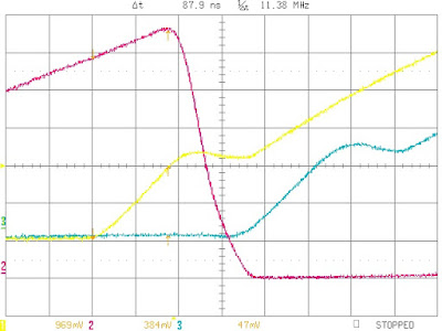
I ran a simulation, probed the S1, S2, and S3 nets, and zoomed into the area where S1 rises, S2 falls, and eventually S3 rises. Here's what it looked like:


It's hard to judge from just the graph, but the time from when S1 begins to rise until S2 begins to fall is about 88ns. This is the phase which represents Cgs charging. If our model is correct, we should see the same behavior on the breadboard:


Well, what a surprise! The simulation matches the model. This suggests that the simulation models Phase A pretty well. What happens after that, in Phase B, is not so good, but that's fodder for another post.

[Edit: I've been asked several times to email the SPICE model I used. It can be downloaded from this link.]

Monday, November 21, 2016

Another attempt at simulation

I really haven't been in the mood to finish any of the PCB layouts, but I didn't want to let this project languish untouched. One of the items on my list has been to get valid simulation results so I can predict whether my choice of pull-up resistors is valid.

In the interim there's been an update to the published Spice model for the FDV301N MOSFET. One of the changes was to change the Cgs value from 78pf to 8.5pf, which makes much more sense to me. I re-ran the simulation from June 2012, and found the new model reduced the per-stage propagation delay from about 200ns to 105ns. This is an improvement, but still longer than the 70ns or so I'm seeing on the breadboard when the effects of the scope probe loading is factored out.

I'm still comparing the simulation results with the actual tracings to understand what needs tweaking to make the simulation more accurate. To make it easier to understand this rather complex model I drew the FDV301N model using the LTspice schematic capture:


The resulting netlist differs from the original model only in comments and minor formatting; otherwise it's identical right down to the net names. I no longer wonder why simulations using this model are so slow.

In the process I think I've discovered an error: the negative output of the EDB voltage source is connected to net 0 (ground), which makes no sense given that the positive output is connected via diode D to the FET's drain pin.  It seems to me that only things related to the temperature input (net 50) should be referenced to ground. I don't think this is affecting the test simulations, since all the Source pins (net 30) are connected to ground, but it would affect some of my real circuits.

Monday, May 23, 2016

Choosing an FPGA for board six

I've been thinking a lot about a sixth board to support an FPGA to assist in debugging and emulating the rest of a complete system (like a Busicom calculator). I'll still put a connector on the I/O & Timing board so the CPU can be interfaced directly to external logic, but having the ability to access inter-board signals and emulate missing parts of the CPU seems worth the effort.

When I first started this project, I used a Xilinx Spartan-3E FPGA development board for this, but it only provided 40 I/O signals. I thought about building my own board with the same FPGA, but it seemed a bit pricey and complicated to interface (three supply voltages with rigid power-up timings, etc). Thus I looked around and found the Lattice iCE40-HX series.

In the years since I started this project, the FPGA world has changed. Xilinx came out with their Spartan-6 series, which can run with two voltage supplies without stringent order or rise-time criteria. The parts have also become denser and cheaper ($16 vs $22). The iCE40-HX4K is still a bit less than half that price ($7), but when considering the cost of the PCB and the components required to support the FPGA (voltage regulators, SPI Flash ROM, level-shifting FETs) the difference in the cost of the FPGAs is noise.

I've decided to use the Xilinx Spartan-6 LX9 (144-pin TQFP) rather than the iCE40-HX4K. Why? In a word: Tools. I'm much more familiar with the Xilinx tool chain, and the iSIM simulator runs under Linux. The Aldec simulator provided by Lattice is a fine tool, but it only runs under Windows.

I need to finish pinning out all four remaining boards before I lay out the debug board, but I'm almost finished creating the Eagle library parts I'll use, and have most of the other components selected.

Friday, April 15, 2016

M-32TL operation notes

I took a brief look at the M-32TL printer in my Canon P170-DH calculator. I haven't figured out all the details, but here's what I've learned so far.

Wednesday, April 13, 2016

A VFD module for the calculator?

One of the problems with converting a stock calculator to emulate a Busicom 141-PF is that most calculators these days max out at 12 digits, while the 141-PF was a 15-digit calculator. The example Tim McNerney gives in his PIC-based printer emulator test data is:
//                   111111 1 1
//          123456789012345 7 8
/* ============================= */
/*          3.1415926535897 x    */
/*                        2 =    */
/*          6.2831853071794   *  */
/*                               */
/*                     -456 /    */
/*                     2.37 =    */
/*         -192.40506329113   *  */
/*                               */
/* ============================= */
Thus it's not as simple as dropping a couple of digits to truncate the output to 12 digits. Nor would that account for the two special characters that appear in columns 17 and 18. One way I'm considering handling this is to replace the P170-DH's fluorescent display with an LCD module.

One I'm considering is the CFAH2002A-TMI-JT module from Crystalfontz, a company I've bought from before. This module is a negative transmissive LCD with a blue foreground and white LED backlit characters. This is important because the P170-DH has a blue-colored plastic bezel, and I think this combination is most easily viewable compared to a the typical yellow-green transflective display. It displays two lines of 20 characters each, so I could either show the last two lines printed or display status on the second line. It's fairly inexpensive at about $15, but presents some mounting challenges.


Still, the idea of using a Vacuum Fluorescent Display module has stuck in my head. Most of the VFDs I've found haven't been suitable, but I just came across the DS2029H from Noritake-Itron. Not only does this module appear to be an almost perfect fit for the P170-DH, it's less than $30 in sample quantities from the manufacturer.


Of course VFDs require some strange power supplies (+5Vdc and +35Vdc in this case) but that's manageable. This module includes a controller that looks much the same as those found in LCD modules so I don't need to deal with segment drivers and the like. They also sell VFD modules that look just like LCD modules (including one they're discontinuing that is being sold at only $18), but like the LCD modules they wouldn't fit as well.


Edited to add: I ordered a DS2029H Vacuum Fluorescent Display from Noritake-Itron Wednesday. It just shipped, so I should have something to play with next week.

Tuesday, April 12, 2016

Another reminder to myself

I was reading some old posts to this blog when I came across a good idea that I'd since forgotten: separate the external I/O driver Vdd from the internal logic Vdd. This would allow the external I/Os to be driven to 3.3V instead of 5V, easing the interface to modern electronic components such as FPGAs. I haven't tested this idea on a breadboard yet, but it seems like it ought to work. I'm writing this posting so I don't forget the idea again.

And what about the EP-102? I got it working, mostly. There's a weird hiccup that causes additional lines to be "printed" to the serial port, but I suspect that's a glitch in the test module and not the printer emulation.

I also looked at some LCD and OLED character modules. I'm torn between 20x1, 20x2, and 16x2 modules. The 20x1 would be most readable, but might not fit in the space available. A second line would allow me to display other info like the OVR indicator, along with the characters that should be in columns 17 and 18 in the case of a 16x2. I'm also somewhat constrained by the blue-colored window in the calculator's case.