PCB-Pool has a fun feature called
WATCH"ur"PCB® in which they email you photos of your board at various stages of fabrication. They claim it's to let you make sure the board is being prepared properly, but I think it's just eye candy for hobbyists. Of course I signed up for it!
Any of the pictures can be enlarged by clicking on it.
The first peek at your board-to-be is a PDF with four images of the board. These depict the top mask and silkscreen, the bottom mask and silkscreen, the top copper layer, and the bottom copper layer:
The images in this picture are shown looking through the board from the top side. This is the same view presented by Eagle during board layout. The rest of the pictures in this post are photographs of the actual board in production, so naturally the bottom is viewed from the bottom.
For some reason they don't give you images of the inner layers. This is somewhat annoying, especially since this is my first 4-layer board and I don't happen to have ready access to an X-ray machine to visualize them after the board arrives. Since I've placed a lot of vias in the corners of SMD pads I want thermals for inner layers, and I'm just going to have to trust that I selected the proper option (Eagle shows that I did, but it'd be nice to see it from PCB-Pool too).
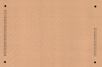
The next step is drilling. There are only three sizes of holes on this board: four large mounting holes in the corners, 104 mid-sized holes for the connector pins, and a gazillion teeny-tiny vias.
 |
| Top |
|
 |
| Bottom |
|
After drilling comes the application of the photo resist. If I understand the process correctly, a photosensitive laminate is applied to the board, exposed and cured. This leaves the areas to be protected from etching exposed.
 |
| Top |
|
 |
| Bottom |
|
|
Tin is then applied to the exposed areas to protect from the copper from the etchant. After etching the tin is removed, leaving bare copper.
 |
| Top |
|
 |
| Bottom |
|
My understanding is that the round dots surrounding my layout are placed in areas on the panel that will be discarded to balance the chemical copper etching process. In any case, they roughly outline my board, but are not part of it.
That's the last of the photos I've received to date. The board must still be coated with a solder mask, silkscreened, and protected from oxidation by the application of chemical tin. This board is just too densely packed to allow for each component's name to be screened on, so I chose to have only component outlines and circuit blocks printed.


No comments:
Post a Comment